International Technology Resource
Systematic Debug
A Production Technician's Guide to Troubleshooting Electronics
Free public review edition - July 2026
Before using this book
This book teaches diagnostic reasoning. It does not authorize electrical work, energized testing, rework, disposition, or deviation from controlled processes.
Work only within your training, qualification, authorization, equipment ratings, applicable law, and employer procedures. Product drawings, specifications, safety analyses, customer requirements, and controlled work instructions take precedence. De-energize exposed hazardous circuits unless an approved exception and qualified-person procedure applies.
This edition is free to read and download. Copyright 2026 International Tech Resource. All rights reserved. Redistribution of the unmodified PDF or EPUB is permitted for noncommercial training with attribution; resale, altered editions, certification claims, and removal of safety notices are prohibited.
Examples and case studies are fictionalized composites unless explicitly sourced. Numerical examples are teaching values, not universal limits.
Introduction
You just got hired at a contract electronics manufacturer. Maybe it's your first job out of trade school. Maybe you transferred from a different line. Maybe you've been soldering for years but never sat at a debug station.
On your first day, someone hands you a board that failed functional test. There's a traveler clipped to the ESD bag. The test log says "OUTPUT LOW — CHANNEL 3." The board is a design you've never seen before, for a product you've never used, built to a spec the customer wrote. Nobody on your shift designed this thing. Nobody on your shift has ever talked to the customer's engineers.1
Determine what the evidence supports and route the board correctly.
Sometimes that ends in repair. Sometimes it ends in retest, containment, escalation, no-defect-found with an explanation, or an authorized scrap decision. This book teaches the diagnostic work that makes that disposition defensible.
What This Book Is
This is a troubleshooting methodology book. It teaches you how to think through failures systematically — how to receive a board, assess it, form a hypothesis, test it, and reach root cause without wasting time or burning through components.
The setting is a contract electronics manufacturing floor. The examples are production PCBAs. The tools are what you'll find at a real debug station. But the thinking method applies far beyond electronics — it's a structured approach to diagnosing any system where something isn't working the way it should.
Unless otherwise cited, the measurements, board names, reference designators, customer details, production histories, troubleshooting heuristics, and case-study narratives in this book are original or fictionalized composite material created for training. They are meant to teach diagnostic reasoning, not document a specific employer, customer product, failure lot, manufacturer test result, or formal standard.2
What This Book Is Not
This is not an electronics theory textbook. It assumes you know the basics — what a resistor does, what voltage is, how to read a schematic at a basic level. If you need that foundation, there are excellent books for it (Platt's Make: Electronics and Scherz's Practical Electronics for Inventors are good starting points).
This is not a repair guide for consumer products. You won't find instructions for fixing your TV or your phone. Those books exist. This one is for the production floor.
This is not a soldering or certification manual. Rework must be performed only by personnel authorized and qualified under the site's controlled process. IPC training and standards may be part of that system, but this book does not grant certification or acceptance authority.3
Who This Book Is For
- New technicians sitting at a debug station for the first time
- Experienced techs who learned by tribal knowledge and want to formalize their process
- Training managers looking for a structured onboarding resource
- Students in vocational or community college electronics programs who want to know what the job actually looks like
How This Book Works
There is a master flowchart at the core of this book. It covers the complete troubleshooting process from the moment a failed board reaches your station to the moment it leaves with a disposition. Every chapter in this book maps to a section of that flowchart.
You can read the book front to back to build the full methodology. You can also flip to a specific chapter mid-shift when you're stuck at a particular stage of debug. The flowchart tells you where you are. The chapter tells you what to do next.
Part 1 teaches the mindset — the thinking principles that experienced troubleshooters use instinctively but rarely explain out loud. Part 2 covers the systematic frameworks — specific methods for isolating faults. Part 3 walks through the tools and what they actually tell you. Part 4 catalogs the common failure modes you'll encounter. Part 5 covers how your work fits into the production floor around you. Part 6 puts it all together with case studies walked through start to finish.
A Note on Organizational Differences
Every company does things a little differently. Some shops let techs scrap boards on their own judgment. Some require quality sign-off on every disposition. Some have dedicated rework stations. Some expect the debug tech to do their own rework. Some customers provide full schematics. Some provide almost nothing.
This book teaches the process and the thinking. Your company defines the authority and the specific procedures. Where organizational responsibilities come into play, the book will note it — but it won't pretend to know your particular shop's rules.
The Flowchart
Turn to Chapter 1. It starts there.
Sources and notes
- Fictionalized opening scenario created for this manuscript. It is not based on a specific employer, customer, board, or test log.
- Editorial provenance note for this manuscript. Use real schematics, BOMs, datasheets, customer specifications, site procedures, standards, and safety requirements when applying these examples to a production board.
- IPC/electronics.org, "IPC J-STD-001J Requirements for Soldered Electrical and Electronic Assemblies," accessed 2026-04-22, https://www.electronics.org/meet-your-standards.
Before You Begin: Safety, ESD, and Precautions
Read this section before you set foot at a debug station. Before the methodology. Before the tools. Before the flowchart. None of it matters if you hurt yourself or destroy the board you're trying to fix.
This is the short version. Chapters 2 and 3 go deeper. But if you read nothing else on your first day, read this.
Personal Safety
Electricity can kill you. Most production boards operate at low voltage and the risk is minimal, but power supplies, motor drivers, and anything connected to mains voltage can carry lethal energy. Capacitors can hold charge after power is removed, so treat stored energy as a live hazard until you have verified otherwise.3
Before you work on any board:
- Know what voltage is on it. Read the documentation. If the board handles mains voltage or has high-voltage sections, verify those areas are de-energized before probing. Use a meter to confirm — don't assume.
- De-energize hazardous circuits before working near exposed conductors. Energized testing is not an entry-level workaround. It belongs only to people qualified for that equipment, using the site's written energized-work procedure, specified PPE, insulated tools, and properly rated test equipment. If those controls are not in place, stop and escalate.3
- Wear safety glasses when soldering, desoldering, or using hot air. Solder spatters. Flux pops. Components can crack and eject fragments.
- Don't touch hot things. Soldering irons are 300-400°C. Hot air stations blow 350°C+ air. Boards fresh from rework are hot. Freshly desoldered components are hot. Give them time.
- Work in ventilated areas. Solder fumes and flux fumes are irritants. Leaded solder requires hand washing after handling. If your station doesn't have fume extraction, request it.
- Know where the first aid kit and emergency shutoff are. Before you need them.
Electrostatic Discharge (ESD)
ESD is invisible, silent, and destroys semiconductors. You can carry static charge far above the withstand voltage of sensitive components without noticing it. Many electronic components are susceptible below 100 volts, and common bench/static-generation scenarios can reach thousands of volts.1 You are a walking ESD generator — especially in dry environments, on carpet, wearing synthetic clothing.
The damage ESD causes is insidious. It doesn't always kill a component outright. It can weaken it — degrade a junction, thin an oxide layer — so the part passes test today and fails in the field six months from now. This is commonly described as latent ESD damage: earlier ESD exposure may leave a device degraded while it continues to function for some period of normal operation.1
Every time you are at the debug station:
- Wear your wrist strap. Connected to the mat or a verified ground point. Not dangling loose. Not in your pocket. On your wrist, snug, connected. Test it at the start of every shift if your station has a tester.
- Work on the ESD mat. The board goes on the mat. Tools go on the mat. Nothing floats around on the bare bench surface.2
- Handle boards by the edges. Don't touch components, pins, or connector contacts with bare fingers.
- Use ESD-safe bags and totes for transport. Pink poly bags are static dissipative. Shielded (silver/black) bags provide better protection. Regular plastic bags generate static — never use them for boards.2
- Verify your grounding connection before picking up a board. A brief touch is not a substitute for the site's continuous personnel-grounding method. Reconnect and retest your wrist strap or footwear system whenever you return to the station.
If this feels excessive, remember that a mishandled assembly can become a latent field failure rather than a simple bench repair. The short routine of grounding yourself and controlling the work surface is cheap compared with chasing an avoidable failure later.1
Protecting the Board
The board you're debugging is not yours. It belongs to a customer, it has value, and your job is to return it in better condition than you received it — not worse. Every action you take at the debug station has the potential to introduce new damage if you're not careful.
Power-up protection:
- Do not improvise a power-up. Use the approved source, connection, sequencing, voltage, and current profile for that assembly. A bench supply is appropriate only when the product documentation or an authorized test plan permits it. Chapter 17 explains how to choose and configure the source.
- Treat current limiting as protection, not diagnosis by itself. Constant-current operation means only that demand exceeded the set limit. A short is one possibility; normal inrush, startup load, or an incorrectly low limit are others. If behavior differs from the approved profile, remove power and investigate before changing the limit.
Handling protection:
- Support the board. Don't let it flex, bow, or twist. Don't clamp it with excessive force. PCB substrate cracks under mechanical stress, severing internal traces you can't see or repair.
- Be careful with probes. Probe tips can slip and short adjacent pins or scratch through solder mask to expose copper. Use fine-tip probes appropriate for the pitch of the components you're probing. Don't jab.
- Don't stack boards. Components on the bottom board get crushed by the weight of the top board.
Rework protection:
- Use the right temperature. Too much heat lifts pads, damages components, and delaminates the board. Too little heat makes cold joints.
- Protect adjacent components. When using hot air to remove a component, nearby parts can reflow and shift. Use shielding (aluminum tape, silicone shields) when working near sensitive neighbors.
- Clean according to the controlled process. Flux chemistry, coating, customer requirements, and the approved rework procedure determine whether and how residues are removed. Do not apply an unapproved solvent or cleaning step to a customer assembly.
Documentation Protection
One more thing to protect: the chain of information.
- Log when you receive the board. Time, serial number, your initials.
- Log what you find. What you saw, what you measured, what you did.
- Log the disposition. What happened to the board when it left your station.
If you skip this, you haven't just failed to document — you've created a traceability gap. In regulated industries (medical, automotive, aerospace), traceability gaps trigger audits, holds, and investigations that are orders of magnitude more expensive than the board you were trying to fix.
Write it down. Every time.
This is the foundation. Everything in this book builds on it. The methodology only works if you and the board both survive the process intact.
Now turn to Chapter 1.
Sources and notes
- EOS/ESD Association, "EOS/ESD Fundamentals Part 1: An Introduction to ESD," accessed 2026-04-21, https://www.esda.org/esd-overview/esd-fundamentals/part-1-an-introduction-to-esd/.
- EOS/ESD Association, "ANSI/ESD S20.20-2021," accessed 2026-04-22, https://www.esda.org/store/standards/product/314/ansiesd-s20-20-2021/.
- Virginia Tech Environmental Health & Safety, "Capacitors," accessed 2026-04-23, https://ehs.vt.edu/programs/occupational-safety/electrical-safety-in-research-operations/capacitors.html; OSHA, "Control of Hazardous Energy: Lockout/Tagout," accessed 2026-04-23, https://www.osha.gov/sites/default/files/publications/OSHA3120.pdf.
Chapter 1: The Master Flowchart
This chapter is the spine of the book. Everything else hangs off it.
The flowchart on the facing page (and in the pullout card at the back of the book) shows the complete troubleshooting process for a failed board at a debug station. It's the same process whether you're debugging a two-layer consumer board or a twelve-layer aerospace assembly. The details change. The structure doesn't.
Memorize this flow. Not because someone will quiz you, but because when you're three hours into a shift and staring at a board that makes no sense, this structure keeps you from chasing your own tail.
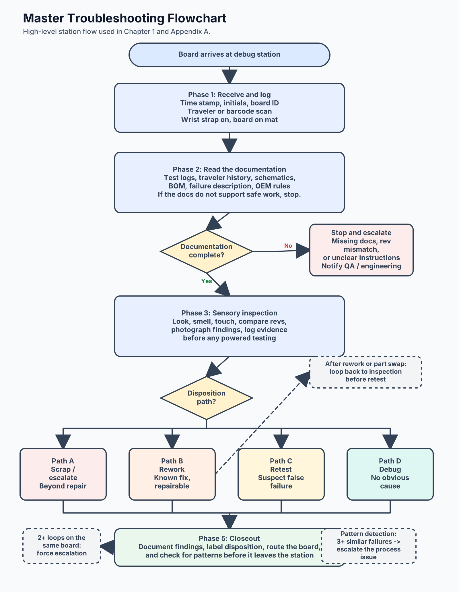
The Five Phases
Phase 1: Receive and Log
The board arrives. It's in an ESD bag (or it should be), with paperwork — a traveler, test logs, maybe a failure description from the test operator.1
Before you do anything else:
- Log the receipt. Time stamp. Your initials. Board serial number or barcode scan. This is traceability. If this board shows up in a customer audit six months from now, someone needs to know who touched it and when.
- Put on your ESD wrist strap. Connect to the mat. The board goes on the mat. This isn't optional and it isn't ceremonial. ESD damage is real, invisible, and capable of creating intermittent or latent failures.2
Phase 2: Read the Documentation
Read everything that came with the board. All of it. Before you touch a probe, before you plug anything in, before you even look closely at the board.
- Test logs: What test did it fail? What station? What were the measured values versus the expected values? If the log says "Pin 14 voltage: 1.2V, expected: 3.3V," you already know where to start looking.
- Traveler: Has this board been here before? Was it reworked already? How many times? What was done? A board on its third trip to debug is a different problem than a first-time failure.
- Failure description: What did the test operator observe? Sometimes this is detailed. Sometimes it says "FAIL." Either way, read it.
- Schematics and BOM: If available, understand the board's function. What does this product do? Where does the failed circuit fit in the overall design? You don't need to understand every gate and trace — you need to understand the block diagram. Power comes in here. Signal flows this way. Output goes there.
- OEM notes and special instructions: Some customers have specific debug procedures, rework limits, or "do not touch" zones. Violate these and you create a much bigger problem than the one you're trying to fix.
If documentation is missing or incomplete, stop. Escalate to your lead, QA, or engineering. You cannot debug effectively without knowing what the board is supposed to do and how it failed. Guessing wastes time and risks further damage.
This step feels slow. It isn't. The five minutes you spend reading saves thirty minutes of directionless probing.
Phase 3: Sensory Inspection
Now inspect the board without energizing or mechanically stressing it. Use your eyes first. Note an odor only if it is already apparent at normal working distance; never lean in to sniff a failed assembly.
Look. Good lighting, magnification if you have it. You're scanning for anything visually wrong:
- Solder bridges between pins
- Tombstoned components (one end lifted off the pad)
- Missing components (empty pads where the BOM says something should be)
- Wrong components (doesn't match the reference designator or silkscreen marking)
- Reversed polarity (electrolytic caps, diodes, ICs rotated 180 degrees)
- Bent or bridged pins on fine-pitch ICs
- Lifted pads or traces
- Cracked board substrate
- Excessive or insufficient flux residue
- Physical damage — scratches, dents, gouges, signs of mishandling
- Board revision marking doesn't match the documentation
Notice unexpected odor safely. An acrid or ozone-like odor already present at the station can indicate overheating, vented material, or arcing. Do not localize it with your nose. Isolate the assembly, ventilate as required, and use visual inspection, approved imaging, and instruments after the hazard is assessed.3
Check mechanical condition without adding damage. With the board de-energized, supported, and inside the site's ESD controls, verify connector seating and inspect mounting points. Do not rock components, bend the board, scrape surfaces, or press on suspect joints unless an approved diagnostic procedure provides a fixture, limits, and authorization.
Listen. This one waits for powered testing. But when you do power up, listen for:
- Arcing (sharp snapping or buzzing)
- Whining or buzzing from inductors or capacitors (can indicate oscillation or saturation)
- Clicking from relays that should be static
Document what you find. Photograph everything. Write it in the log. Even if you think it's minor. A flux splash you noted on Board 47 might be the same flux splash on Boards 48 through 63, and that pattern is worth more than any single fix.
Phase 4: The Disposition Decision
Based on what you've read and what you've seen, make a call. You're sorting the board into one of four paths:
Path A — Scrap. The board is damaged beyond reasonable repair. Cracked substrate with severed traces. Multiple catastrophic component failures. Customer's rework limit already exceeded. This board is done. Tag it, document why, and route it for QA review.
Path B — Rework. You found a clear workmanship or process defect that you can fix. Solder bridge you can wick. Missing component you can place. Tombstone you can reflow. The defect is identified, the fix is known, and you can execute it (or hand it to a rework tech who can).
Path C — Retest. Something doesn't add up. The failure description doesn't match what you see. The test logs show a marginal value that might just be fixture wear or calibration drift. The board looks clean. Before you debug a phantom, verify that the test was valid. Rerun it. Check the fixture. Check the tester calibration. Many boards at the debug station aren't actually broken — they were tested incorrectly.
Path D — Debug. No obvious defect from inspection. The test failure is real. The board needs component-level diagnosis. This is where the rest of the book takes over.
Most of the time, you'll know within a few minutes which path you're on. If you do not, choose the least intrusive authorized check that can resolve the uncertainty. A retest is appropriate only when the board has passed the required safety and inspection gates and the tester, fixture, and procedure are approved for that assembly.
Phase 5: Closeout
Every path ends here. No board leaves your station without documentation.
- Update the traveler or MES system: what you found, what you did, what the result was
- Label the board with its disposition and your initials
- Route it: back to the line, to rework, to scrap, to hold — wherever it needs to go
- Check for recurrence: is this failure appearing across a shared lot, line, fixture, panel position, or time window? Follow the site's reaction plan or alert the responsible lead or quality contact with the evidence you have.
The Feedback Loops
The flowchart isn't purely linear. Three feedback loops run through it constantly:
1. Pattern Detection. After every board, ask: have I seen this before, and what do the units share? Do not wait for a universal count. One safety-critical anomaly may require immediate containment; several ordinary failures may still be random. Use the product's reaction plan, control limits, severity, and shared-factor evidence to decide when to escalate.
2. Re-entry After Repair. After any rework or component replacement, you don't go straight to retest. You loop back to sensory inspection. Did your fix introduce something new? Did the hot air damage an adjacent component? Is the new solder joint clean? Verify before you test.
3. Escalation Awareness. Escalate when you reach the site's time, rework, uncertainty, or authority boundary; when evidence contradicts the documentation; or when the next step could damage the assembly. A fixed number of loops is not a universal rule. Record what has been checked so the next person can continue from evidence rather than repeat the same work.
Using the Flowchart on the Floor
The pullout card at the back of this book is designed to be laminated and pinned to your debug station. Use it. Not because you'll forget the steps — after a few weeks, you won't — but because it keeps you honest. When you're tired, when you're rushing, when you've got fifteen boards in the queue and your lead is asking for status, the flowchart prevents you from skipping the step that would have caught the problem in two minutes instead of twenty.
The chapters that follow expand each section of this flowchart into the detail you need to execute it. Chapters 2 and 3 cover safety and ESD.4 Chapter 4 goes deep on documentation. Chapter 5 covers sensory inspection. Chapters 6 through 9 teach the thinking principles that separate a methodical troubleshooter from a random poker. Parts 2 through 6 handle the tools, the failures, and the floor.
Start with the flowchart. Always come back to the flowchart.
Sources and notes
- EOS/ESD Association, "ANSI/ESD S20.20-2021," accessed 2026-04-22, https://www.esda.org/store/standards/product/314/ansiesd-s20-20-2021/.
- EOS/ESD Association, "EOS/ESD Fundamentals Part 1: An Introduction to ESD," accessed 2026-04-22, https://www.esda.org/esd-overview/esd-fundamentals/part-1-an-introduction-to-esd/.
- Odor is an incidental warning cue, not an instruction to inhale near a failed assembly. Follow the site's chemical, electrical, ventilation, and incident-response procedures before further inspection.
- Safety and ESD source families used in those chapters include OSHA, "Control of Hazardous Energy: Lockout/Tagout," accessed 2026-04-23, https://www.osha.gov/sites/default/files/publications/OSHA3120.pdf; and EOS/ESD Association, "EOS/ESD Fundamentals Part 1: An Introduction to ESD," accessed 2026-04-22, https://www.esda.org/esd-overview/esd-fundamentals/part-1-an-introduction-to-esd/. Actual bench procedures must follow the site's safety rules, equipment documentation, and applicable regulations.
Chapter 2: Safety on the Production Floor
A good troubleshooter is useful only if they can keep themselves, the board, and the people around them safe. The debug station looks quiet compared to the production line. No conveyor, no oven, no feeder banks. But the bench has its own hazards: stored energy, live probing, hot tools, sharp leads, chemicals, fumes, and the temptation to skip a precaution because the queue is full.
Do not treat safety as a separate training module you finish before the real work starts. Safety is part of the troubleshooting method. The process in this book assumes you can slow down long enough to understand what is energized, what can burn you, what can poison the board, and what can create a traceability problem.
This chapter is not a replacement for your company's safety training. Your site procedures, customer requirements, and local regulations control what you are allowed to do. The goal here is to make the safety decisions visible so you can recognize them before they become incidents.2
2.1 Electrical Hazards
Most production PCBAs are low voltage. That does not mean harmless. A low-voltage board can still carry enough current to vaporize a probe tip, burn a trace, or destroy a component. Power supplies, motor controllers, lighting drivers, industrial controls, and anything connected to mains voltage can carry lethal energy.3
Before you apply power or touch a probe to a board, answer four questions:
- What voltage enters the board?
- Which sections stay energized after input power is removed?
- Where are the high-current paths?
- What test points can be probed safely without slipping into adjacent pins?
Capacitors deserve special attention. Bulk capacitors in offline power supplies and motor drives can hold charge long after the board is unplugged. A qualified person must follow the approved discharge and verification procedure with suitably rated test equipment. Do not assume that elapsed time or an indicator lamp establishes a safe state.
De-energization is the default around exposed hazardous conductors. Energized testing is allowed only when the employer's procedure determines that it is necessary and assigns it to a qualified person trained for the equipment and hazard. That procedure must define the boundaries, PPE, insulated tools, probe setup, guarding, and emergency controls. The informal "one-hand rule" is not a substitute for those controls.5
2.2 Chemical Hazards
Flux, solder, isopropyl alcohol, conformal-coating removers, adhesives, and cleaning agents all belong at real debug stations. They are useful, and they need respect.
Flux fumes are irritants. Leaded solder requires hand washing after handling. Isopropyl alcohol is flammable and dries skin. Some coating removers and solvents are much harsher than IPA and require specific gloves, ventilation, and disposal procedures.
Use the safety data sheet for the material in front of you. Do not guess from smell. Do not mix cleaners because "both are used on boards." Keep caps closed when not in use, label secondary containers, and keep chemicals away from energized equipment unless the procedure explicitly calls for their use.
2.3 Physical Hazards
The debug station has many small ways to hurt you.
Cut leads and trimmed component legs are sharp. Connector shells and board edges can cut skin. Soldering irons, hot air nozzles, preheaters, and freshly reworked components stay hot after you stop paying attention to them. Compressed air can drive debris into eyes. Board fixtures and clamps can pinch fingers or crack boards if forced.
Wear safety glasses during rework, clipping, cleaning, scraping, and hot-air work. Treat every iron as hot. Park tools in their holders, not on the mat. Give parts time to cool before picking them up. If a component must be held while heating, use tweezers or a fixture, not fingertips.
2.4 PPE Requirements
Personal protective equipment is not a badge. It is the minimum layer between you and predictable hazards.
At a typical debug station, expect:
- Safety glasses for rework, clipping, cleaning, and any work where fragments or liquid can move toward your face.
- ESD wrist strap and ESD-safe footwear or floor treatment as required by the site.1
- Heat-resistant handling tools for hot boards or recently reworked components.
- Gloves when handling chemicals that require them, and no gloves where they create snag or contamination risk.
Gloves are not automatically safer. Loose gloves near rotating tools, small fixtures, or hot-air work can create new problems. Follow the site rule for the specific task.
2.5 Lockout and Test Equipment Awareness
Some debug work happens on boards alone. Some happens inside fixtures, test racks, powered harnesses, environmental chambers, or customer equipment. Once the board is part of a larger system, the hazards change.
Before reaching into a fixture:
- Know what supplies the fixture applies.
- Know whether motion, pneumatic clamps, heaters, or relays can activate.
- Know how to shut it down.
- Know who is allowed to service it.
Lockout/tagout is usually associated with larger equipment, but the principle matters here too: if unexpected energization or motion can hurt someone, do not rely on memory or a sticky note. Follow the site's control procedure.4
2.6 Ergonomics
Bad bench habits produce slow injuries. Long shifts under magnification, repeated wrist rotation, bent-neck microscope work, and awkward probing angles all add up.
Set up the station so the board is stable and your hands are supported. Bring the work to your eyes instead of folding your neck down to the work. Use the microscope height adjustment. Use board holders when they reduce hand strain. Take short eye breaks during long inspection sessions. Good ergonomics is not comfort for its own sake; it keeps your hands steadier and your judgment sharper.
2.7 Emergency Protocols
Before you start a shift, know:
- Where the emergency shutoff is.
- Where the first aid kit is.
- Where the eyewash station is, if chemicals are used nearby.
- How to report an injury, near miss, electrical incident, or chemical spill.
- Who has authority to clear equipment after an incident.
Do not hide near misses. A probe slip that arcs but does not injure anyone is still data. A fixture that pinches a cable today can pinch a finger tomorrow. Reporting is how the line gets safer before someone pays for the lesson.
2.8 The Safety-First Culture
Production pressure is real. The queue is visible. Leads ask for status. Customers want shipments. That pressure is exactly why the safety habit has to be built into the process instead of added when convenient.
The safe path is usually the efficient path. Reading the voltage notes before probing prevents blown boards. A correctly configured current limit bounds available current while you compare behavior with the approved startup profile. Proper ventilation keeps the station usable. Logging hazards prevents the next tech from repeating your surprise.
The debug station rewards calm, repeatable behavior. Safety is the first repeatable behavior.
Key Takeaway
Safety is not separate from troubleshooting. It is the condition that makes troubleshooting possible. Know the energy on the board, control the tools and chemicals around you, respect fixtures and live circuits, and document hazards just like you document failures. A board can be replaced. A person cannot.
Sources and notes
- EOS/ESD Association, "ANSI/ESD S20.20-2021," accessed 2026-04-22, https://www.esda.org/store/standards/product/314/ansiesd-s20-20-2021/.
- OSHA, "Control of Hazardous Energy: Lockout/Tagout," accessed 2026-04-23, https://www.osha.gov/sites/default/files/publications/OSHA3120.pdf. This book provides general awareness only; site procedures and applicable regulations control actual work.
- Virginia Tech Environmental Health & Safety, "Capacitors," accessed 2026-04-23, https://ehs.vt.edu/programs/occupational-safety/electrical-safety-in-research-operations/capacitors.html.
- OSHA, "1910.147 - The control of hazardous energy (lockout/tagout)," accessed 2026-04-23, https://www.osha.gov/laws-regs/regulations/standardnumber/1910/1910.147.
- OSHA, "Electrical Safety-Related Work Practices - Inspection Procedures and Interpretation Guidelines," accessed 2026-07-18, https://www.osha.gov/enforcement/directives/std-01-16-007; OSHA, "Training and PPE for employees performing tests on equipment," accessed 2026-07-18, https://www.osha.gov/laws-regs/standardinterpretations/1998-06-22-0. OSHA requires exposed live parts to be de-energized unless the employer can justify an allowed exception; only qualified persons may perform testing on energized circuits or equipment.
Chapter 3: ESD - The Invisible Killer
Electrostatic discharge is one of the most frustrating failure sources in electronics manufacturing because it often leaves no visible mark. The board looks clean. The solder joints look good. The component may even pass test today. Then it fails next week, next month, or after it reaches the customer.
That delayed failure is why ESD belongs near the front of this book. It is not just a handling rule. It is a troubleshooting reality. ESD damage can be catastrophic or latent, and latent damage may not be caught immediately by ordinary production test.1 Those failures consume debug time and confuse root cause analysis.
3.1 What ESD Actually Does
Static charge builds when materials contact and separate: shoes on flooring, clothing against a chair, plastic packaging against a bench. The EOS/ESD Association's examples show that ordinary workplace actions can generate hundreds to thousands of volts depending on humidity and materials.1 Many semiconductor structures are damaged at voltages far below the threshold of human sensation.
Inside an IC, ESD can cause oxide failure, junction breakdown, metal melt, or other damage mechanisms.1 The part may die instantly, or it may be wounded. A wounded part is worse from a quality perspective because it can pass production test and fail later under heat, vibration, voltage margin, or normal aging.
This is why "I did not feel a shock" means almost nothing. You are not the measuring instrument. The silicon is.
3.2 Latent Failures
A hard ESD failure is easy to understand: the component is dead, the board fails, and debug finds the failed part.1
A latent ESD failure is more expensive. The component still functions, but its margin is reduced. A MOSFET gate leaks slightly more than it should. A comparator input develops offset. A microcontroller pin becomes sensitive to temperature. A communication transceiver works at room temperature but fails after thermal soak. Treat these as plausible failure signatures to verify, not as proof of ESD by themselves.1
From the debug station, latent ESD damage may look like:1
- Intermittent communication errors.
- Boards that fail only at temperature or only after warm-up.
- A batch of parts from one handling step showing unexplained failures.
- Functional failures with clean solder, correct BOM, and normal passive measurements.
- Components that fail again after replacement if the handling problem remains.
When you see a failure pattern that does not fit the visible hardware, include ESD handling in your hypotheses.1
3.3 The ESD-Protected Workstation
An ESD-protected station creates a controlled path for charge to equalize slowly instead of discharging suddenly through a component. ANSI/ESD S20.20 provides administrative and technical requirements for formal ESD control programs.2
The basic station includes:2
- A grounded ESD mat.
- A wrist strap connected to the mat or a verified ground point.
- ESD-safe tools where required.
- Dissipative or shielded bags and totes.
- Grounded shelves, carts, or fixtures when boards move between stations.
- Ionization where insulators cannot be removed from the work area.
The details vary by facility, but the principle does not: every conductive item that can touch the board should be at the same electrical potential, and insulators that can hold charge should be controlled or kept away.
Test your wrist strap at the start of the shift if the station has a tester. A strap clipped to nothing is decoration. A strap worn over a sleeve may not contact skin. A mat with a broken ground cord is just a rubber sheet.
3.4 Handling Protocols
Good ESD behavior is boring because it is repeated every time.2
Before touching a board:
- Put on the wrist strap.
- Verify it is connected.
- Place the board on the ESD mat.
- Handle the board by the edges.
- Keep regular plastic, foam, tape, and loose packaging away from exposed assemblies.
Use the right packaging. Pink poly bags are static dissipative but do not provide the same shielding as metallized bags. Shielded bags protect assemblies during transport because charge stays on the outside of the bag. Regular plastic bags generate and hold static; they do not belong around exposed PCBAs.
Moving boards between stations is a common weak point. The board leaves the protected bench, rides in a tote, sits near a fixture, gets handled by another operator, then returns to debug. ESD control has to cover the handoff, not just the bench where the failure is found.
3.5 Common ESD Mistakes
New techs usually understand the rule. The mistakes happen in small exceptions:2
- Wearing the wrist strap but not plugging it in.
- Clipping the strap to painted metal or an unverified point.
- Handling boards by connector contacts because it is convenient.
- Setting a board on paperwork, foam, bubble wrap, or a bare cart.
- Pulling a board from a shielded bag before the bag is on the mat.
- Using non-ESD brushes or wipes that generate charge.
- Letting visitors or operators hand boards across the bench without grounding.
Each exception feels small. The problem is that ESD damage does not announce itself. You may not know which exception caused the failure until a pattern emerges later.
3.6 Recognizing ESD Damage Patterns During Debug
You cannot usually look at a part and say, "This was ESD." You infer it from the pattern and the absence of better explanations.1
ESD should move up your hypothesis list when:1
- Failures cluster around exposed connectors, user-accessible pins, MOSFET gates, communication transceivers, ADC inputs, or comparator inputs.
- The same component type fails across multiple boards with no solder or BOM defect.
- Failures correlate with a station, shift, fixture, handling step, dry weather, or packaging change.
- Replacement parts fix the board, but only if handled from verified ESD-safe stock.
- The electrical symptom is leakage, offset, marginal timing, or temperature sensitivity rather than a clean open or short.
Document the handling context along with the electrical finding. "U12 failed" is useful. "U12 input leakage high on four boards handled at rework station 3 after mat ground failed test" is root-cause evidence.
3.7 ESD Myths
"If I did not feel it, it did not happen." False. Human sensation starts far above the damage threshold of many devices.1
"The board is already failed, so ESD does not matter." False. You can add new damage while investigating the original failure, making diagnosis harder and potentially destroying evidence.1
"Foam is safe." Only if it is the right ESD-safe foam and in good condition. Random packing foam is often a charge generator.2
"Humidity solves ESD." Higher humidity helps reduce charge buildup, but it does not replace grounding, packaging, and controlled handling.2
"One strap at one station protects the whole process." False. The board is only protected while the handling environment is controlled.
Key Takeaway
ESD is invisible, silent, and expensive. It can create immediate failures, and it can also leave damage that is difficult to detect immediately.1 Treat ESD control as part of troubleshooting discipline. Ground yourself, control the work surface, use proper packaging, watch for handling patterns, and document suspected ESD evidence clearly enough that quality or process engineering can act on it.
Sources and notes
- EOS/ESD Association, "EOS/ESD Fundamentals Part 1: An Introduction to ESD," accessed 2026-04-21, https://www.esda.org/esd-overview/esd-fundamentals/part-1-an-introduction-to-esd/.
- EOS/ESD Association, "ANSI/ESD S20.20-2021," accessed 2026-04-21, https://www.esda.org/store/standards/product/314/ansiesd-s20-20-2021/.
Chapter 4: Read Before You Touch
The most common mistake a new tech makes at the debug station has nothing to do with a multimeter. It's picking up a probe before picking up the paperwork.
Every failed board that reaches your station arrives with information. Sometimes a lot. Sometimes barely any. But whatever is there, it was generated by the systems and people upstream of you — the test station, the operator, the MES system, the customer's documentation package. That information is your starting advantage. Ignoring it is like starting a jigsaw puzzle by throwing away the picture on the box.
What Comes With the Board
The Test Log
This is the most immediately useful document at your station. It tells you what test the board ran, what it measured, and where the measurement went wrong.
A good test log gives you specific pins, specific values, and specific limits. "Pin 14 measured 1.2V. Expected range: 3.0V to 3.6V." That's a starting point. You already know where to put your probe first.
A bad test log says "FAIL" and nothing else. This happens more often than it should. When it does, you need to look at the test station's data system or talk to the test operator before proceeding. Debugging without knowing the failure mode is like driving without knowing the destination — you'll move, but not usefully.
Pay attention to:
- Which specific test step failed. A board that fails step 3 of 200 is a different animal than one that fails step 197.
- Measured values versus limits. A measurement that's slightly outside the window might be a marginal part or fixture drift. A measurement that's wildly out of range (0V where you expected 5V) points to a hard failure.
- Multiple failures versus single. A board that fails one test might have one problem. A board that fails twelve tests might have a power rail down — one root cause knocking out everything downstream.
The Traveler
The traveler (or work order, or routing sheet — every shop calls it something different) is the board's history. It tells you where this board has been and what's been done to it.
Critical questions the traveler answers:
- Is this the board's first trip to debug? A first-time failure is normal. A third-time failure means two previous attempts didn't find the root cause — or created new problems.
- What rework was previously performed? If someone already replaced U14 last week, and the board is back with the same symptom, U14 probably wasn't the real problem. Or the replacement was defective. Or the rework introduced damage.
- What's the board's build history? Which line built it? Which shift? What date? This matters for pattern detection — if every board from Line 2 on Tuesday is failing the same test, the problem isn't the boards.
Schematics and Design Documentation
Not every customer provides schematics to the CM. Some guard their IP fiercely and give you nothing but a test fixture and a pass/fail result. Others hand you full design packages. Most fall somewhere in between.
When you have schematics:
- Don't try to understand the entire design. Find the section relevant to the failure. If the test log says the 3.3V rail is low, find the 3.3V regulator circuit on the schematic. Trace its input, output, and feedback path. That's your world for the next thirty minutes.
- Check the BOM revision against the board. Mismatches between the schematic rev and the board rev cause phantom problems that can't be debugged because the documentation doesn't match reality.
When you don't have schematics:
- You're relying on the test log, visual inspection, and comparison to a known-good board. This is harder but not impossible. It just means your golden board (Chapter 7) becomes even more critical.
OEM Special Instructions
Some customers include debug procedures specific to their product. Read them. They may include:
- Maximum number of allowed reworks before the board must be scrapped
- Specific components that must not be reworked (potted areas, sealed modules)
- Required debug sequences ("always check firmware version before hardware debug")
- Approved replacement parts list (you can't always substitute from your general stock)
Violating controlled instructions can create contractual, quality-system, regulatory, safety, and traceability problems far beyond the debug station. The applicable requirements depend on the product, customer, jurisdiction, and employer's quality system.
What to Do When Documentation Is Missing
It happens. The ESD bag arrives with a board and nothing else. No traveler. No test log. No failure description. Someone dropped it off and walked away.1
Do not guess. Do not assume. Do not "just take a look."
Escalate immediately. Find the production lead, the test operator, or QA. Get the documentation. If it can't be found, that itself is a quality issue that needs to be logged.
There are two reasons for this:
- You can't troubleshoot effectively without knowing the failure mode. You'll waste time testing things that aren't broken.
- Traceability. If you work on a board with no documentation trail, and that board ends up in a customer's product, and that product fails in the field, the audit trail is broken. In regulated industries, that's a serious problem.
The five minutes it takes to track down the paperwork is not wasted time. It's the most efficient thing you'll do all day.
Building Your Own Documentation
Everything you read when the board arrives, someone upstream wrote. As a debug tech, you are also writing documentation — for the next person. Maybe it's the rework tech. Maybe it's the quality engineer. Maybe it's yourself, two weeks from now, when the same board comes back.
Get in the habit now:
- Note the time you start. Note the time you finish.
- Write down what the test log said before you did anything.
- Write down what your visual inspection found.
- Write down every measurement you take and where you took it.
- Write down your hypothesis and what you did to test it.
- Write down the result — whether it confirmed or refuted your hypothesis.
This feels tedious. It isn't. It's the difference between a technician who fixes boards and a technician who makes the whole line better. Your documentation is the raw data that feeds pattern detection, root cause analysis, and process improvement. Without it, every board is an island. With it, you're building a map.
Sources and notes
- Fictionalized training scenario created for this manuscript. It illustrates a documentation gap rather than a specific real incident.
Chapter 5: Use Your Senses
Inspection starts before the instruments, but observation must not create a new exposure or a new defect.
Before you power up a board, before you connect a meter, before you touch a probe to a test point — inspect the board with your own senses. This isn't a quick glance. This is a deliberate, systematic examination that catches problems no instrument would find as fast.
Visible heat damage or a reversed IC can redirect a debug session immediately. An unexpected odor already apparent at the station is a warning to isolate and assess the assembly, not an invitation to inhale more closely. Mechanical checks must use approved fixtures or procedures, not fingertips and board bending.
The sensory inspection is not preliminary. It is diagnostic.
Look
Eyesight is your primary inspection tool. Use good lighting — overhead fluorescents aren't enough for fine-pitch work. A task light angled across the board creates shadows that reveal solder defects. Magnification helps: a loupe, a stereo microscope, or even your phone camera zoomed in.
Work systematically. Don't just glance at the board and declare it clean. Start at one corner and scan across, row by row, like reading a page. Check both sides.
What You're Looking For
Solder defects. These are a frequent production failure category in CM environments.
- Bridges: Solder connecting two pads or pins that shouldn't be connected. Common on fine-pitch QFPs and SOICs. Under magnification, they're obvious. Without magnification, they hide.
- Cold joints: Dull, grainy, or cracked solder instead of smooth and shiny. The joint looks formed but isn't making reliable contact. These create intermittent connections that pass one test and fail the next.
- Voids and insufficient solder: Pad is visible through a thin solder coat, or the fillet is incomplete. Component may be electrically connected but mechanically weak.
- Tombstones: One end of a passive component (resistor or cap) has lifted off its pad, standing up like a tombstone. Usually a reflow issue. Electrically, it's either an open or an intermittent.
Component issues.
- Missing components: An empty pad pair where the BOM says something should be. Compare to the assembly drawing or a known-good board.
- Wrong components: The marking doesn't match the reference designator. A 10K resistor where the BOM calls for 1K. A 10uF cap where a 100nF should be. These are placement errors from the pick-and-place machine.
- Reversed polarity: Electrolytic caps, diodes, and ICs can be placed backwards. Check the polarity marking against the silkscreen or assembly drawing. A reversed electrolytic can fail violently. A reversed IC will simply not work — or will work briefly and then die.
- Bent or misaligned pins: Especially on fine-pitch QFPs and connectors. A pin folded under the package makes no contact. A pin bent sideways bridges to its neighbor.
Board-level damage.
- Cracks in the substrate: Can sever internal traces. Often caused by mechanical stress — panel depaneling, fixture clamping, or handling.
- Lifted pads or traces: Copper peeling from the board surface, usually from excessive heat during previous rework or from mechanical force.
- Scratches or gouges: May have cut through a trace. Hold the board at an angle and look for bright copper lines where the solder mask is scraped away.
Contamination.
- Excessive flux residue: Can be conductive under humidity, causing leakage paths between traces. Also obscures solder joints from visual inspection.
- Foreign material: Solder balls, wire clippings, or debris trapped under components or between pins.
Documentation mismatch.
- Board revision: The silkscreen revision marking should match the traveler and the documentation package. If it doesn't, you may be looking at a schematic that doesn't represent what's actually on the board.
Notice Odor Without Sniffing
An unexpected odor can be useful incident information, but deliberate sniffing near damaged electronics can expose you to irritating or hazardous decomposition products.
An acrid odor already apparent at normal working distance can indicate overheated material or a vented component. Remove power if applicable, isolate the assembly, and follow the site's ventilation and incident procedure. Localize the damage with visual inspection, approved imaging, and instruments after the hazard is assessed.
An ozone-like odor can accompany electrical discharge. Treat it as a stop signal: de-energize through the approved method and have the energized section assessed by a qualified person.
Flux and cleaning residues vary, and odor alone cannot identify when or why a material was heated. Record the observation without assigning a root cause.
Mechanical Inspection
Keep the assembly de-energized, supported, and inside the site's ESD controls. Use the assembly drawing, magnification, approved gauges, and a board holder or diagnostic fixture where needed.1
Connectors. Verify seating, latch position, housing condition, and visible solder joints. Do not use connector movement alone to condemn a joint; confirm the finding visually or electrically under an approved test.
Components and laminate. Do not rock packages, press suspect joints, run a finger across damaged material, or flex the board by hand. Those actions can crack MLCCs, extend laminate damage, disturb intermittent evidence, contaminate surfaces, or convert a marginal assembly into a new failure.
Listen
Hearing comes into play during powered testing, which is later in the process. But it's worth covering here because the sensory inspection mindset extends into every phase.
When an authorized powered test is underway under Chapter 17's controls, listen from the normal operating position.
Sharp clicking, snapping, or unexpected buzzing can indicate electrical discharge or a mechanical switching problem. Remove power through the approved method and escalate before another attempt.
Inductor whine is a high-pitched tone, sometimes audible only to younger ears. It can indicate an inductor operating in saturation, an unstable switching regulator, or a feedback loop oscillating. Compare to the sound (or silence) of the same area on a known-good board.
Capacitor whine from MLCCs (multi-layer ceramic capacitors) is caused by piezoelectric effects under AC voltage. Some amount is normal in certain designs. If it's new — present on the failed board but not on the good one — it's telling you something is oscillating that shouldn't be.
Relay clicking when relays should be stable, or silence when a relay should be energizing, are immediate functional indicators.
The Discipline of Documentation
Everything you find during sensory inspection gets recorded. Not after debug. Not at the end of the shift. Now.
- Photograph solder defects, physical damage, and anything unusual with a site-approved imaging device. Personal phones may be prohibited where customer designs, controlled data, or export restrictions apply.
- Note locations by reference designator (e.g., "Solder bridge between pins 3-4 of U7") rather than vague descriptions.
- Note what you didn't find, too. "Visual inspection: no defects observed" is useful because it tells the next person in the process that inspection was performed and was clean.
A sensory inspection that isn't documented didn't happen. And findings you document today become pattern data tomorrow — when the fourth board from the same batch shows up with the same solder bridge on the same IC, your notes are what triggers the escalation that catches the upstream process problem.
When Inspection Finds Nothing
Sometimes the board looks perfect. No defects. No smell. No loose parts. Everything appears correct.
That's fine. It just means the failure isn't visible — it's internal to a component, it's a marginal parametric issue, or it's a design-edge condition. You've ruled out the easy wins and now you proceed to debug with that knowledge. The clean inspection is data. It tells you the problem is likely electrical, not mechanical or workmanship-related.
Proceed to the disposition decision (Chapter 1, Phase 4) and continue from there.
Sources and notes
- EOS/ESD Association, "ANSI/ESD S20.20-2021," accessed 2026-04-22, https://www.esda.org/store/standards/product/314/ansiesd-s20-20-2021/.
Chapter 6: The Failure Chain
You find a burnt resistor. Blackened. Maybe a hole through it. Obvious failure. Your instinct says: replace the resistor, retest, move on.
Don't.
That resistor is the victim. Something killed it. If you replace it without finding what, you're reloading the gun and pulling the trigger again. The board will come back — same failure, or a new victim nearby, because the actual cause is still sitting on the board, quietly out of spec, waiting.
This chapter teaches the single most important principle in component-level troubleshooting: the component that burns is the weakest part of the circuit, not necessarily the broken one.
How Failure Chains Work
Current flows through paths. Components in those paths have ratings — maximum voltage, maximum current, maximum power dissipation, maximum temperature. When conditions exceed those ratings, something gives. The component that gives first is the one with the least margin between its rating and the abuse it's taking.
But the abuse has a source. Something upstream created the overcurrent, the overvoltage, or the thermal condition that killed the visible victim. And something downstream may also have been damaged before the weakest link finally gave way.
A failure chain looks like this:
Root cause (upstream) → overcurrent/overvoltage condition → weakest component burns (what you see) → possible downstream damage (what you might not see yet)
Real Examples
| What You See | What Actually Happened |
|---|---|
| Burnt current-sense resistor | A MOSFET downstream failed short, pulling unlimited current through the sense resistor until it burned open |
| Fried MCU | The voltage regulator feeding it lost regulation and output 9V into a 3.3V part |
| Blown protection diode | A transistor in the drive circuit failed short, reverse-biasing the diode beyond its rating |
| Scorched trace | A solder bridge elsewhere created a short-circuit path through a trace not designed for that current |
| Vented electrolytic capacitor | Reverse polarity from an assembly error — the cap was installed backwards and the electrolyte boiled |
In each case, replacing the visible failure without addressing the cause would result in a repeat failure.
The Rule: Trace Backward Before You Replace
When you find a damaged component, treat it as your entry point into the circuit — not your diagnosis. You need to answer four questions before you replace anything:
1. What killed this part?
Determine the failure mechanism. A burnt resistor died from overcurrent (too much current through it, exceeding its power rating). A fried IC died from overvoltage (voltage on a pin exceeded the absolute maximum rating). A cracked capacitor might have died from thermal stress or voltage exceeding its rating.
The failure mechanism tells you what kind of condition to look for upstream.
2. Where did those conditions come from?
Trace the circuit path backward from the dead component. What feeds it? What regulates the voltage or limits the current to that part of the circuit?
If a resistor burned from overcurrent, what's on the other end of it? If the answer is "a MOSFET that switches a load," check the MOSFET. Is it shorted? Is the load drawing more current than designed?
If an IC died from overvoltage, what supplies its power pin? Is the regulator outputting the correct voltage? Check it — not with the dead IC in circuit (it may be loading the rail down), but by understanding the designed voltage and verifying the regulator's behavior.
3. Are the upstream parts still in spec?
Don't just check whether upstream components are obviously dead. Check whether they're still within their specifications. A regulator that's outputting 3.5V instead of 3.3V might be technically "working" but that extra 200mV, combined with temperature and tolerance stacking, pushed the downstream part over its limit.
A capacitor that reads the correct capacitance but has elevated ESR (equivalent series resistance) might be causing voltage ripple that stresses downstream components during transient loads.
Use your golden board (Chapter 7) for comparison. What do the upstream components measure on the working unit? If there's a difference, even a small one, that's your lead.
4. Are there downstream casualties?
The failure condition existed before the weakest link blew. During that time, the overcurrent or overvoltage condition was also present on other components in the path. Some of them may have been damaged but not destroyed — degraded, weakened, shifted in value.
Check downstream components the same way you checked upstream. Measure them. Compare them to the golden board. A component that survived the event but was stressed may fail next week under normal operation.
The Swap-and-Pray Trap
Here's what happens when you skip the failure chain analysis:
- Board arrives. Burnt resistor R47 on the 12V rail.
- Tech replaces R47. Board powers up. Passes functional test.
- Board goes back to production. Ships to customer.
- Two weeks later: Field return. Same board. R47 is burnt again.
- Board comes back to debug. Tech replaces R47 again. Maybe scratches head. Ships again.
- Third return. Now the customer is angry. Now quality is involved. Now it's a big deal.
The root cause was Q3, a MOSFET that was intermittently failing short under thermal load. It was there the whole time. Each time R47 was replaced, Q3 was still failing intermittently, pulling destructive current through R47 until it burned again. If the tech had traced backward from R47 on the first occurrence, they'd have found Q3 and fixed both parts. One trip to debug instead of three. One shipment instead of three returns.
Swap-and-pray doesn't save time. It multiplies the time by the number of returns.
The Practical Procedure
When you find a visibly damaged component:
FOUND DAMAGED COMPONENT
         |
         v
  DO NOT REPLACE YET
         |
         v
  Identify the failure mechanism
  (overcurrent / overvoltage / thermal)
         |
         v
  Trace the circuit path BACKWARD
  from the damaged component
         |
         v
  Check every upstream component:
  - Is it in spec?
  - Does it match the golden board?
  - Is the voltage/current at its output correct?
         |
         v
  Check downstream components too:
  - Were they exposed to the same abuse?
  - Are they still in spec?
  - Are any degraded but not dead?
         |
         v
  Root cause identified?
    |              |
   YES             NO
    |              |
    v              v
  Replace        Escalate with
  BOTH the       documentation of
  root cause     what you checked
  AND the        and what you
  victim         found
    |
    v
  Retest the FULL circuit path
  Not just the component you replaced
When the Chain Is Longer Than You Think
Sometimes the failure chain has more than two links. A failed regulator killed an IC, and the IC's failure shorted a bus that damaged two other ICs on the same bus. You replace the regulator and the first IC but miss the bus damage. The board passes basic functional test because those other ICs were only handling an edge case — and then it fails in the field when that edge case occurs.
This is why the downstream check matters. And it's why comparison to a known-good board (Chapter 7) is so valuable. If you probe every component in the affected circuit path and compare to the golden board, you catch the third and fourth links in the chain.
Key Takeaway
The burnt component tells you where to start looking. It does not tell you what's wrong. A methodical tech treats visible damage as the beginning of the investigation, not the end. Trace backward. Check upstream. Check downstream. Fix the cause and the victim. Retest the path, not just the part.
This is the difference between a parts swapper and a troubleshooter.
Chapter 7: The Golden Board
Ask a new tech what reading they got on a test point and they'll tell you "2.7 volts." Ask them if that's correct and they'll shrug.
That's the problem. A measurement without a reference is just a number. Two-point-seven volts means nothing until you know whether it's supposed to be 2.7 volts. Troubleshooting is not absolute measurement. It is comparison.
A controlled reference assembly can make measurements far more informative. It does not turn every difference into a defect, and it does not replace the schematic, specifications, calibration, or engineering judgment. It provides a product-specific comparison when its identity and condition are known.
Why You Need One
In a contract manufacturing environment, you're debugging boards you didn't design for customers you may never talk to. You might have schematics. You might not. You might have a test spec with expected values at specific test points. You might not.
If you have an approved reference of the same revision and configuration, you can compare corresponding nodes under controlled conditions. The schematic and test specification remain authoritative: an uncontrolled reference can contain undocumented variation, and two matching boards can still both be wrong.
A golden board is especially critical when:
- You've never seen this product before. New product introduction (NPI) builds are exactly when failures are most common and documentation is least mature.
- Schematics are unavailable or restricted. Some OEM customers provide minimal documentation for IP protection.
- The failure doesn't match documented test points. The problem might be in a section of the circuit that the test spec doesn't cover.
- You're chasing an intermittent. Comparing behavior over time between a good board and a flaky one reveals patterns that absolute measurements miss.
Where to Get One
In order of preference:
1. Identical Known-Good Unit
Same product, board revision, approved BOM configuration, firmware, and relevant options. Its identity and passing status are recorded. When corresponding nodes are measured under the same setup, it provides a strong product-specific comparison.1
Sources: First-article boards from the production run. Pilot builds that passed all testing. Ask your production lead or engineering if one is available.
2. Functionally Similar Unit
Same product, different board revision or minor BOM changes. The core design is the same — same MCU, same power architecture, same major functional blocks — but some component values or layout details may differ.
This may still be useful when engineering identifies which blocks and conditions are comparable. Do not assume rails, clocks, thresholds, or startup behavior match across revisions; check the change record and applicable specifications first.
3. Schematics with Expected Values
When no physical reference exists, you fall back to the documentation. Schematics tell you what the circuit is designed to do. Test specs give you expected values at specific points.
Specifications and design documentation define acceptance; a reference assembly adds observed behavior. Use both. A measured value inside an approved range is not a failure merely because it differs from one reference, and a matching value is not proof that all requirements are met.
4. Your Own Measurement Log
Over time, controlled measurements from verified assemblies can build a useful baseline. Store them in the approved system with product revision, firmware, fixture, instrument, settings, environmental conditions, and date. A private notebook without configuration control is a lead, not an acceptance standard.
What You Can Do With a Golden Board
Passive Comparison (Unpowered)
This is the most underused technique in production debug, and it might be the most valuable.
With both boards powered off, measure resistance or capacitance at the same nodes on both boards. Use your multimeter's resistance range or an LCR meter.
- A shorted capacitor on the failed board reads near zero ohms where the good board reads the expected impedance.
- An open trace on the failed board reads infinite resistance where the good board shows continuity.
- A failed semiconductor junction reads differently on a diode test than its counterpart on the good board.
The advantage of this technique is that it can narrow differences without energizing the failed board. Use identical meter polarity, range, settling time, and connection points. Stored charge and alternate return paths still require the safety and discharge controls in Chapter 2.
Work systematically. Start with the power rails (measure resistance from each supply rail to ground on both boards). Then check the area around the reported failure. Differences between the two boards are your leads.
Voltage Mapping (Powered)
Power each board only through its authorized setup and compare equivalent operating states. Do not improvise a shared supply, load, or grounding arrangement merely to put two boards side by side.
- The 3.3V rail reads 3.31V on the good board and 2.81V on the failed board. That 500mV difference is your flag — something is loading down that rail or the regulator is failing.
- A bias voltage reads 1.65V on the good board and 0V on the failed board. Follow that voltage to its source.
- An output reads 4.98V on both boards. That one operating-point measurement agrees; it does not by itself clear the entire section.
Voltage mapping is methodical and fast. You're not guessing where to look. You're scanning for differences and chasing the ones you find.
Signal Comparison (Scope)
First confirm the scope input ratings, probe ratings, board references, isolation, and grounding. Earth-referenced probe grounds can short nodes or join two systems through the oscilloscope. When the setup is safe and authorized, compare corresponding waveforms sequentially or simultaneously as the test plan permits.3
The waveforms overlay. Where they match, the circuit is behaving identically. Where they diverge — different amplitude, different timing, different shape, or signal present on one and absent on the other — you've found your area of interest.
This is particularly useful for:
- Clock signals: Is the frequency the same? Is the waveform clean or noisy?
- Switching regulators: Is the switching waveform present? Same duty cycle?
- Communication buses: Is the data pattern the same? Is there ringing or reflections on one board but not the other?
Thermal Comparison
With an approved thermal-imaging setup, compare the assemblies at the same load, elapsed time, airflow, ambient temperature, surface condition, and viewing geometry.
A working board establishes the baseline thermal profile — which components run warm, which run cool, where the hot spots normally are. A component that's significantly hotter on the failed board than on the good board is working harder than it should — possibly because of a fault in its circuit, possibly because it's the fault itself.
A component that's cold on the failed board but warm on the good board isn't running at all — possibly because it's not getting power, not getting a signal, or is dead.
When You Don't Have a Golden Board
This happens. Especially during NPI (new product introduction) when there may not be any passing units yet, or when the customer can't or won't provide one.
Your options:
- Ask for one. Directly. Tell your lead or engineering that debug efficiency depends on having a reference unit. Production usually has first-articles or pilot boards set aside for exactly this purpose.
- Ask engineering or quality to establish one. A passing unit does not become a controlled reference merely because a technician labels it. The owner should verify its configuration, record its status, define permitted uses, and place it under change and storage control.2
- Fall back to documentation. Use schematics and test specs. Accept the limitation and document it: "Debug performed without known-good reference. Diagnosis based on schematic expected values."
Whichever path you take, note it in your debug documentation. If a diagnosis turns out to be wrong later, the absence of a golden board may be a contributing factor.
Taking Care of the Golden Board
A golden board that gets damaged, modified, or contaminated is worse than no golden board — it gives you wrong comparisons.
- Store it in an ESD bag when not in use.2
- Identify it clearly with product, revision, configuration, firmware, reference status, owner, and verification date.
- Never rework it. Never use it for parts. Never "borrow" a component from it.
- Verify it at the interval and by the method defined by its owner; do not invent a universal monthly interval.
- When the product or approved configuration changes, evaluate whether the reference must be revised, requalified, or retired.
Key Takeaway
A measurement gains meaning from requirements and controlled comparison. A verified reference assembly can help isolate differences, especially when documentation is limited, but it does not define acceptance by itself. Know its configuration, reproduce the setup, record differences, and interpret them against the product documentation.
Sources and notes
- Original troubleshooting method guidance. Specific voltage values in examples are fictional unless tied to a real product datasheet or test specification.
- EOS/ESD Association, "ANSI/ESD S20.20-2021," accessed 2026-04-22, https://www.esda.org/store/standards/product/314/ansiesd-s20-20-2021/.
- Tektronix, "ABCs of Probes," grounding and probe-safety guidance, accessed 2026-07-18, https://www.tek.com/en/documents/primer/abcs-probes-primer.
Chapter 8: Trust Nothing on the Board
You've checked the solder joints. You've traced the failure chain. You've compared against the golden board. The hardware checks out. Every component measures in spec. Every connection tests good. The board still fails.
Before you escalate, before you declare it a mystery, ask one more question:
Is what's on this board actually what's supposed to be on this board?
The schematic can be right. The layout can be right. The soldering can be right. The component itself can still be wrong — not defective in the traditional sense, but wrong for this application. Wrong firmware. Wrong silicon. Wrong provenance.
This chapter covers three failure sources that live outside conventional hardware debug. They're invisible to a multimeter. They don't show up on visual inspection. And they waste more debug hours than most techs realize, because nobody thinks to check for them until everything else has been exhausted.
Firmware Revision Mismatches
A microcontroller, FPGA, EEPROM, or any programmable device on the board runs code. That code has a version number. The board was designed and tested against a specific version of that code. If the chip is running a different version, the board may fail functional test even though every piece of hardware is perfect.
How This Happens
- OEM rev control mismatch. The customer sent firmware v2.3 for production, but the BOM still references v2.1. The programming station loaded what was in the system.
- Supplier pre-programmed with old firmware. Some chips come from the vendor with firmware already loaded. If the vendor's stock is older, the firmware is older.
- Mixed inventory. The stockroom has two reels of the same MCU. One reel was programmed for the previous build lot. The pick-and-place machine doesn't know the difference.
- Programming station error. The firmware file on the programming station was never updated. Every board this week got the old firmware.
What the Tech Sees
The board powers up. It partially works. Some functions pass, some don't. Or it boots to a different state than expected. Or it communicates but with wrong protocol timing. Or it passes every electrical test but fails the final functional/application test.
The symptoms are confusing because the hardware is fine. The tech chases phantom component failures because that's what they're trained to look for.
What to Do
When hardware debug comes up clean and the board fails functionally:
- Check the firmware version. Many programmable devices have a register or command that reports their firmware revision. If the board boots far enough for communication (JTAG, UART, SPI, USB), query it.
- Check the programming log. The programming station should have a log of what firmware file was loaded onto each board by serial number. Compare the logged version to the version in the current build documentation.
- Compare to the golden board. If the golden board runs firmware v2.3 and the failed board runs v2.1, you've found your problem.
- Reflash and retest. If the firmware is wrong, reprogram the device with the correct version and retest. If it passes, log the root cause as a firmware mismatch and notify whoever manages the programming station.
This is a five-minute check. It should be part of your standard debug procedure for any board with programmable devices, performed before you spend an hour probing passives.
Counterfeit Components
Counterfeit and nonconforming electronic components are a recognized supply-chain risk. A counterfeit component may have the right markings on the outside but the wrong or inferior die on the inside. It may have been pulled from scrap boards and re-marked, manufactured by an unauthorized source, or sold with fraudulent labeling.1
How Counterfeits Enter the Supply Chain
- Broker purchases. When a part goes on allocation or end-of-life, CMs sometimes buy from brokers on the open market instead of authorized distributors. Brokers don't always verify authenticity.
- Unauthorized or undisclosed substitution. A supplier ships a different part, grade, revision, or source without the approvals and traceability required by the purchase documents. That is a nonconformance and a supply-chain concern; it is not, by itself, proof of counterfeiting.
- Salvage and remark. Components are desoldered from discarded boards, cleaned up, re-tinned, and re-marked with current date codes. The silicon might be damaged from the original removal, aged, or a lower-spec version.
What the Tech Sees
Counterfeit components can behave in baffling ways:
- The part reads in-spec on the bench (correct resistance, correct capacitance, correct forward voltage) but fails in the circuit. The parametric specs match but the dynamic behavior doesn't — switching speed, noise floor, or transient response is wrong because it's a different die.
- The board works at room temperature but fails at the edges of the operating temperature range. The genuine part was rated for the full range. The counterfeit isn't.
- Multiple boards from the same build lot fail in the same way, centered on one specific component. The failure pattern doesn't match any known defect mode for that component.
- Swapping the suspect component with one from a different source (e.g., a sample from an authorized distributor) fixes the problem.
Screening Observations During Visual Inspection
Train your eyes for these during the sensory inspection phase:
| What to Look For | Why It's Suspicious |
|---|---|
| Marking style, position, or durability differs from controlled manufacturer or known-good references | The difference may justify specialist examination, but marking processes vary; it is not a stand-alone authenticity test. Do not apply solvents unless an approved inspection procedure authorizes a destructive or semi-destructive test. |
| Date or lot codes conflict with labels, traceability records, or the approved configuration | Mixed codes can occur for legitimate reasons, including repackaging and distributor consolidation. Treat the discrepancy as a traceability question, not proof of fraud. |
| Package surface finish differs from controlled references | Resurfacing is one possible explanation; normal mold-compound, site, date, and process variation are others. Record the observation and compare like-for-like samples. |
| Lead finish or package condition suggests prior handling or rework | This may indicate salvage, poor storage, repacking, or process damage. Preserve the part and traceability evidence for qualified review. |
| Logo, font, or code format conflicts with current manufacturer guidance | Compare with manufacturer documentation and an authenticated sample. Visual appearance alone does not establish die identity or provenance. |
What to Do
If you suspect counterfeits:
- Document everything. Photos of the suspect parts, lot codes, date codes, reel labels, and distributor information.
- Preserve evidence. Do not clean, scrape, open, electrically overstress, or otherwise alter suspect material unless the approved investigation plan calls for it. Retain packaging, labels, paperwork, and chain-of-custody information.
- Pull authenticated comparison samples. Quality or supply-chain personnel may obtain parts from an authorized source for controlled visual, electrical, X-ray, material, or laboratory comparison.
- Escalate to QA and supply chain. This is not a debug-station-level fix. It may require quarantine, supplier investigation, specialist testing, and customer or regulatory notification under the organization's procedure.
- Do not attempt to "make it work." A circuit tweak is not an acceptable disposition for suspect or unauthorized material.
The tech's role is detection and escalation. You're not expected to run a full failure analysis lab on the suspect part. You're expected to recognize the pattern ("multiple boards, same part, doesn't make sense") and raise the flag with evidence.
Silicon Revisions and Die Variations
The same part number on the same datasheet, ordered from the same authorized distributor, can behave differently — because the silicon inside has changed.
How This Happens
Semiconductor manufacturers revise designs, processes, assembly sites, test flows, and fabrication sources. Approved revisions are still expected to meet the published specification, but a marginal design or unvalidated application can react to behavior that legitimately varies within that specification. Relevant changes may be documented through errata, revision identifiers, or product-change notifications.
These changes are usually documented in errata sheets or product change notifications (PCNs). Sometimes they're not. Sometimes the PCN was sent to the OEM's design engineers six months ago and never made it to the CM's production floor.
What the Tech Sees
- Boards fail intermittently or at the margins. Nine out of ten pass. One fails. Swap the IC from the failing board with one from a passing board and the problem moves with the chip — or it disappears.
- A product that ran fine for months suddenly starts showing yield drops after a new shipment of components arrives.
- Timing-sensitive circuits (high-speed buses, ADC sampling, PLL lock times) fail on some boards but not others, with no other variable.
- The failure only manifests under specific conditions — temperature, load, speed — that stress the edges of the part's specifications.
What to Do
- Document the lot codes and date codes on components from failing boards. Also document them from passing boards.
- Look for correlation. If every failing board has chips from lot 2024-W47 and every passing board has chips from lot 2024-W31, you've found a pattern.
- Check for errata. The silicon manufacturer's website may have an errata document listing known issues with specific steppings. This requires knowing the stepping code, which may be printed on the part or readable via JTAG/device ID registers.
- Check for PCNs (Product Change Notifications). The manufacturer or distributor may have issued a notification about a process change. Your engineering team should have received these.
- Escalate with data. Present the lot code correlation to engineering. They can engage with the component manufacturer for clarification. This isn't something the debug tech resolves — it requires design-level and supply-chain-level investigation.
The tech doesn't need to understand the silicon errata. The tech needs to recognize the pattern — "same part, different lot, different behavior" — and hand it off with clean data.
The Common Thread
All three of these failure sources share one characteristic: the hardware looks correct. Visual inspection is clean. Solder joints are good. Components are present and properly placed. Electrical measurements may be in spec. And the board still fails.
This is why "Trust Nothing on the Board" comes after the hardware-focused chapters. It's the next question you ask when hardware debug reaches a dead end:
- Is the firmware correct for this build?
- Are the components genuine?
- Is the silicon revision consistent with what works?
These are not daily occurrences. Most boards fail for straightforward reasons — solder defects, component damage, assembly errors. But when the straightforward explanations run out, these are the next places to look. And when they do turn out to be the cause, they tend to affect entire batches, not individual boards — making early detection especially valuable.
Key Takeaway
A component can be the right part number, correctly soldered, and electrically present — and still be the cause of a functional failure. Firmware version, component authenticity, and silicon revision are invisible to a multimeter but real to the circuit. When hardware debug comes up clean, check these before declaring the board a mystery. And when you find a pattern — same lot, same part, same unexplained failure — document it and escalate. You may be the first person to catch a problem that affects an entire production run.
Sources and notes
- ERAI, "Electronic Supply Chain Counterfeit Reporting and Avoidance," accessed 2026-04-23, https://www.erai.com/.
Chapter 9: Reading Schematics for Debug
The board on your station is failing its 3.3V rail. The test log says "U7 VCC low — 1.8V measured, 3.3V expected." Someone hands you a six-sheet schematic PDF and says "find the problem."
You're not here to admire the design. You need to find U7, figure out where its 3.3V comes from, trace that rail back to the regulator, and identify every component between here and there that could be dragging it down. You need to do this in minutes, not hours.
This chapter isn't a schematic theory course. It's a navigation skill set — the minimum you need to use a schematic as a debug tool on the production floor.
9.1 What a Schematic Tells You (And What It Doesn't)
A schematic shows you the designer's intent. It tells you what components are in the circuit, how they connect, and what function each section is supposed to perform. It's a map of the designed circuit.
What it doesn't tell you:
- The physical layout. Two components next to each other on the schematic might be on opposite sides of the board. The schematic shows electrical connections, not physical proximity. You still need the board (and sometimes the layout drawing) for that.
- Parasitics. Trace resistance, stray capacitance, ground impedance — none of these appear on the schematic, but all of them affect real-world behavior. A long thin trace to a power pin adds resistance the schematic won't show you.
- Actual component values. The schematic shows nominal values. The 100k resistor on paper might measure 97k on the board. That's fine. Or it might measure 120k because of a bad batch (Chapter 13). The schematic can't tell you that.
- Assembly defects. A solder bridge between pins 3 and 4 of a QFN doesn't exist on the schematic. Neither does a tombstoned 0402 capacitor or a cold joint on a BGA.
Use the schematic to understand what should be happening. Use your instruments to find out what is happening. The gap between those two is your fault.
9.2 Identifying Power Rails and Following Them
Power is where you start 90% of the time. A dead or sagging rail kills everything downstream, and the schematic is the fastest way to map out where power goes.
Look for these:
- The main input. Find the connector where power enters the board — usually labeled VIN, VBUS, or with the expected voltage (5V, 12V, 24V). It's often on sheet 1.
- Voltage regulators. Follow the input to the first regulator — an LDO (like an AMS1117-3.3 in SOT-223) or a buck converter (like a TPS62130 in QFN-16). The regulator's output net name tells you the rail designation: 3V3, VCC_3V3, +3.3V, etc.
- The distribution. That output net fans out to every IC and component that needs it. On a complex board, a single 3.3V rail might feed 20 components across four schematic sheets.
- Decoupling capacitors. Every IC power pin should have a bypass cap — typically 100nF 0402 or 0603 — placed close to the pin. These appear on the schematic near each IC but may be grouped on a separate sheet in some designs.
When you're tracing a power problem, you're following that net name across sheets. Every component connected to that net is either a load (drawing current) or a filter/decoupling element. If the rail is low, one of those loads might be pulling it down.
9.3 Tracing Signal Paths from Input to Output
Signals flow. They start somewhere (a sensor, a connector, a processor output) and end somewhere (an actuator, a display, a communications port). The schematic shows that path.
The procedure:
- Find the source. If the failure is "no UART output," find the MCU's UART TX pin on the schematic. If it's "ADC reads zero," find the sensor input.
- Follow the net. The TX pin connects to a net — maybe labeled UART1_TX or just a line running to the next component. Follow it.
- Note every component in the path. A series resistor for impedance matching. A level shifter. An ESD protection diode. A connector. Each one is a potential failure point.1
- End at the destination. The TX line reaches the connector pin that goes off-board, or the RX pin of the receiving IC.
Every component you identified along that path is a candidate for probing. Half-split (Chapter 10) and signal tracing (Chapter 11) both depend on you being able to read this path off the schematic before you touch a probe.
For multi-stage analog paths — say, a sensor amplifier chain — the signal passes through several active stages. Each op-amp or instrumentation amp is a stage. Each filter between stages is a node. Map them all. Your debug will probe each stage boundary looking for where the signal degrades or dies.
9.4 Net Names, Reference Designators, and Cross-Sheet References
Three things you'll read constantly on schematics. Get comfortable with them.
Net names are labels on wires. VCC_3V3, SPI_CLK, RESET_N, PWM_BACKLIGHT. The name tells you the function. A wire labeled the same name on sheet 1 and sheet 4 is the same electrical connection — they're physically connected on the PCB even though they look separate on paper. The _N or _B suffix typically means active-low (the signal does its thing when pulled to ground, not when driven high).
Reference designators identify individual components:
| Prefix | Component |
|---|---|
| R | Resistor |
| C | Capacitor |
| L | Inductor |
| U | Integrated circuit |
| Q | Transistor (BJT or MOSFET) |
| D | Diode (including LEDs) |
| J | Connector |
| Y or X | Crystal oscillator |
| F | Fuse |
| FB | Ferrite bead |
When the test log says "check R47" or "U12 pin 3 low," the reference designator is how you find that component on the schematic and on the board (it's printed on the silkscreen).
Cross-sheet references are arrows, labels, or port symbols at the edge of a schematic sheet that tell you a signal continues on another sheet. They might look like a flag with "Sheet 3, zone B2" or a named port matching a name on another sheet. When you're tracing a signal and it hits one of these, flip to the referenced sheet and find the matching label. Most PDF schematics have clickable cross-references — use them.
9.5 Common Symbols and What They Mean on the Floor
You'll encounter hundreds of schematic symbols over time. Here are the ones you need to recognize immediately at the debug station, and what they mean for your probing:
| Symbol | What It Is | Debug Relevance |
|---|---|---|
| Triangle with +/- inputs | Op-amp | Check supply rails, input bias, output vs expected |
| Rectangle with pin labels | IC (generic) | Read the part number, find the datasheet |
| Zigzag line (or rectangle) | Resistor | Measure in-circuit, compare to marked value |
| Two parallel lines | Capacitor | Check for shorts (especially MLCCs), ESR if you can |
| Coil/loops | Inductor | Check for opens, DCR, saturation under load |
| Triangle with bar | Diode | Diode-test forward voltage, check for shorts |
| Arrow into gate | MOSFET | Gate voltage, drain-source, check for shorts |
| Ground symbols | GND connection | Multiple ground symbols on one schematic are the same net |
| Diamond or filled triangle on power | Power flag | Indicates a net carries power — check it first |
One symbol that trips up new techs: the ground symbol. There might be several different ground symbols on a complex schematic — GND, AGND (analog ground), PGND (power ground), DGND (digital ground). These may or may not be connected on the board. Check. If the board has separate analog and digital ground planes tied at a single point, a solder defect at that tie point creates a ground offset that makes the analog section misbehave.
9.6 Navigating Multi-Sheet Schematics
Production boards rarely fit on one sheet. A typical mid-complexity PCBA — say, an IoT gateway or a motor controller — runs four to twelve sheets. The more sheets, the more you need a navigation strategy.
Start with the table of contents. Most multi-sheet schematics have a title block on each sheet describing its function: "Power Supply," "MCU and Memory," "Ethernet PHY," "Sensor Interface," "Connectors." Find the sheet relevant to your failure.
Use the block diagram if provided. Some design packages include a top-level block diagram showing how the sheets relate. This is gold — it gives you the signal flow between major sections without digging through individual sheets.
Work from the failure backward. If U7's 3.3V is low, go to U7's sheet, find the net name for its VCC pin, and use that net name to jump to the power supply sheet. Don't start on sheet 1 and read forward. Start at the failure and trace back.
Mark up your copy. Print the relevant sheets or annotate the PDF. Highlight the signal path you're tracing. Circle the components you've already probed. Note your measurements. A schematic covered in your handwritten probe values is a debug artifact — it tells the story of what you checked and what you found.
9.7 Working Without Schematics
Some OEM customers won't provide schematics. Intellectual property concerns, contractual restrictions, or simple disorganization. You're expected to debug the board anyway.
Your options, in order:
Ask again. Ask your lead, who asks the program manager, who asks the customer. Frame it as a productivity issue: "Debug time per board is 3x longer without schematics." Sometimes the answer changes when management sees the cost.
Use the golden board (Chapter 7). Passive comparison becomes your primary method. Probe the same points on both boards and look for differences. You don't need the schematic to know that 0 ohms where the good board reads 4.7k is wrong.
Trace the board manually. Follow copper traces visually with a magnifying glass, use continuity mode to map connections, read IC part numbers and pull datasheets to understand pinouts. This is slow, but it builds a functional schematic in your head (or on paper) as you go.
Read component markings. Every resistor, capacitor, and IC has a marking. Read the IC part numbers, look up their datasheets, and work backward from the typical application circuit in the datasheet. Most designs follow the reference design closely. If the datasheet for a TPS62130 shows a typical circuit with specific inductor and capacitor values, and the board has that part, the surrounding components probably match that reference design.
Document what you find. When you figure out a section of the circuit through manual tracing, write it down. The next tech who gets this board will benefit from your work.
Working without schematics is slower and harder, but it's not impossible. It shifts your approach from schematic-guided to comparison-based and measurement-based. Lean heavily on the golden board.
9.8 Reading the BOM Alongside the Schematic
The bill of materials (BOM) lists every component on the board by reference designator, part number, value, package, and manufacturer. The schematic tells you where and how. The BOM tells you what exactly.
Cross-reference them when:
- Verifying a component value. The schematic shows R47 as 10k. The BOM says R47 is a CRCW060310K0FKEA — that's a Vishay 10k 1% 0603. If you measure R47 and get 100k, either the wrong part was loaded or the resistor has failed. The BOM confirms what should be there.
- Checking for substitutions. Production sometimes approves alternate components. The BOM might list a primary and an alternate with different manufacturer part numbers. If the board has the alternate and it's behaving differently, that's data.
- Identifying unmarked parts. Small passives in 0201 or 0402 packages often have no readable markings. The BOM is the only way to know what that tiny component is supposed to be.
- Matching packages for replacement. You need to swap C23. The schematic says 10uF. But 10uF in what package? The BOM says 0805 MLCC, X5R, 16V rated. You need to match all of those parameters, not just the capacitance.
Keep a printed BOM at the debug station alongside the schematic. When you find a component that doesn't match — wrong value, wrong package, missing entirely — you've found a likely root cause. Log it, verify it against what's physically on the board, and disposition accordingly.
Key Takeaway
A schematic is a debug map, not a textbook. You don't need to understand every design decision — you need to find the power rail feeding the failed section, trace the signal path through it, and identify every component along the way that could be your fault. Learn to navigate by net names and reference designators, work backward from the failure, and always cross-check the BOM against what's physically on the board. When you don't have a schematic, lean on the golden board and manual tracing — slower, but not a dead end.
Sources and notes
- EOS/ESD Association, "EOS/ESD Fundamentals Part 1: An Introduction to ESD," accessed 2026-04-23, https://www.esda.org/esd-overview/esd-fundamentals/part-1-an-introduction-to-esd/. For a real product, verify each protection device and interface component against the schematic, BOM, and manufacturer datasheet.
Chapter 10: Half-Split (Binary Search)
You've got a board with a dead backlight. The path from power input to LEDs runs through six components across three inches of PCB. You could probe every single one, starting at the left and working right. That's seven measurements to find one fault.
Or you could probe the middle first. If the middle is good, the fault is in the second half — three components to check. Probe the middle of that half. Two left. One more probe and you've got it.
Three measurements instead of seven. That's half-split. On a longer chain, the savings get dramatic — a path with thirty components narrows to five probes. This is the single most efficient framework for isolating faults on linear paths, and it's the first structured method you should reach for on the production floor.
10.1 The Concept
Half-split is binary search applied to a circuit path. You divide the suspect path in half, test the midpoint, and eliminate the half that's working. Then you divide the remaining half and repeat. Each probe cuts the problem space by 50%.1
The math is simple: a path with n components takes at most log2(n) probes to isolate the fault. A 16-component chain? Four probes. A 64-component path across a complex power distribution network? Six probes. Compare that to probing every component sequentially — the difference is the difference between a five-minute debug and a thirty-minute one.
The only requirement: the path has to be linear. Signal goes in one end, passes through a sequence of components, and comes out the other end. No branches, no feedback loops. Just a chain.
10.2 When to Use It
Half-split works best on:
- Power distribution paths. Input connector to regulator to filter to load. These are almost always linear.
- Signal chains. Sensor to amp to filter to ADC. Audio input to preamp to gain stage to output driver.
- Multi-stage circuits. Any path where the signal passes through several discrete stages in sequence.
- LED and backlight strings. Power source through driver through resistors through the LEDs themselves.
- Connector-to-connector paths. Input jack through the board to the output jack — especially useful on I/O-heavy boards.
Reach for half-split when you already know what is failing (the test log tells you) and need to find where in the chain the fault lives.
10.3 Step-by-Step Procedure
Here's how to run it at the debug station:
Map the path. Open the schematic (Chapter 9) and trace the signal or power path from source to destination. List every component in order. Write them down or mark up the schematic — you need to see the full chain.
Verify the endpoints. Probe the source — is the input present and correct? Probe the destination — is the output dead or wrong? If the input is already bad, the fault is upstream of your mapped path. If the output is actually fine, recheck the test failure report.
Pick the midpoint. Count the components or nodes in your chain and find the middle. It doesn't have to be exact. Close enough is close enough — you're eliminating halves, not performing surgery.
Probe the midpoint. Power the board with a current-limited supply (Chapter 17). Measure voltage, signal presence, or continuity at the midpoint. Compare to the golden board or the expected value from the schematic.
Evaluate.
- Midpoint good? The fault is downstream. The upstream half is cleared.
- Midpoint bad? The fault is upstream. The downstream half is cleared.
Repeat. Take the remaining suspect half, find its midpoint, probe, evaluate. Keep halving until you're down to one or two components.
Confirm. Once you've isolated a suspect component, verify with a targeted test — resistance measurement, diode test, visual inspection, or comparison to the golden board (Chapter 7).
HALF-SPLIT PROCEDURE
====================

Source ----[A]----[B]----[C]----[D]----[E]----[F]---- Destination
                          ^
                     Probe here first
                          |
              +-----------+-----------+
              |                       |
         Midpoint GOOD           Midpoint BAD
         Fault is D-F            Fault is A-C
              |                       |
         Probe [E]               Probe [B]
              |                       |
         Continue halving...     Continue halving...
10.4 Walked Example: Consumer Thermostat Backlight Failure
A consumer smart thermostat PCBA fails functional test — display backlight doesn't illuminate. The test station flags it and kicks it to your debug queue.
Map the path. From the schematic, the backlight circuit runs:
- 5V buck converter output (TPS62130 in QFN-16) — pin VOUT
- 10 ohm 0603 series resistor (R34) — current sense/filter
- LED driver IC (TPS61165 in SOT-23-6) — VIN pin
- LED driver output — pin 3 (SW)
- PWM control signal from MCU (STM32F103 in LQFP-48) — pin PB9 to driver CTRL (pin 2)
- Backlight LEDs via flex connector (J4)
Verify endpoints. Probe the 5V buck output — reads 5.02V. Good. Check the backlight LEDs at J4 — dead dark. Confirmed failure.
First split — midpoint at driver IC pin 3 (SW output). Should be pulsing at roughly 1.2 MHz when backlight is commanded on. Scope reads flat — no switching activity. The fault is upstream of the LED string, somewhere between the buck output and the driver output.
Second split — check the MCU PWM. Probe PB9 on the STM32F103. Clean 3.3V square wave at the expected duty cycle. MCU is doing its job. So the driver IC is getting its enable signal. The fault is between the buck output and the driver IC's power input.
Third split — probe across R34. 5.02V on the buck side. 0V on the driver side. The 10 ohm resistor has no voltage on its output pad.
Confirm. Measure R34 in-circuit — open. Visual inspection under magnification reveals a hairline crack through the body of the 0603 resistor. Likely cracked during reflow from board flex or improper panel support.
Resolution. Replace R34 with a matching 10 ohm 0603 1%. Retest — backlight illuminates, board passes functional test. Three probes to find the fault. Log root cause as cracked series resistor, flag the reflow profile and panel support for the process engineer.
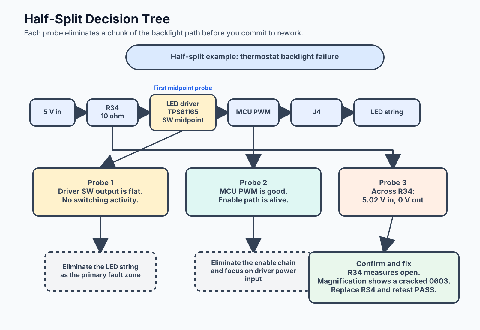
10.5 Adapting for Dense SMT Boards
Half-split is conceptually simple. On a dense board with 0201 passives and QFN ICs on 0.4mm pitch, physically probing the midpoint can be the hard part.
Techniques that help:
- Probe accessible nodes first. Test points, via pads, connector pins, and large component pads are easier to hit. If your ideal midpoint is a buried trace under a shielding can, shift to the nearest accessible node. You lose a little efficiency but keep your sanity and your probe tips.
- Use the golden board's probe points. If you've been building a list of accessible probe points on this product (Chapter 7), you already know where you can land a probe. Choose your midpoints from that list.
- Needle probes over blunt tips. A good set of fine-pitch needle probes reaches individual QFN pads and 0402 component ends that standard multimeter probes can't hit.
- Powered vs. unpowered. For power rail issues, you can sometimes do half-split unpowered — measure resistance to ground at the midpoint and compare to the golden board. A short reads near zero. An open reads infinity. No power-up needed, which is safer and sometimes easier.
- Don't lift pads. On production boards, especially fine-pitch BGA and QFN packages, attempting to probe by prying under components damages the board. If you can't reach a node, skip it and split at the next accessible point. A slightly uneven split still eliminates a large chunk of the problem space.
10.6 Where It Breaks Down
Half-split is powerful but not universal. Know its limits so you don't waste time applying it where it won't work.
Feedback loops. A switching regulator has an output that feeds back to its control input. The output affects the input which affects the output. There's no linear path to split — everything is interconnected. If the output is low, is the feedback loop compensating incorrectly, or is the output stage failing, or is the input stage weak? Half-split can't distinguish these. Use hypothesis-driven diagnosis (Chapter 14) instead.
Non-linear circuits. Circuits where multiple signals combine — multiplexers, logic gates with multiple inputs, bus arbitration. The fault could be on any of several parallel paths feeding a single node. Half-split works on chains, not trees.
Intermittent failures. If the fault comes and goes, your midpoint probe might read good — not because the upstream path is healthy, but because the intermittent isn't active right now. You eliminate the wrong half and chase a ghost. For intermittents, hypothesis-driven diagnosis with environmental stress (temperature, vibration, mechanical flex) is more appropriate.
Very short paths. If the path only has two or three components, half-split is overkill. Just probe them all. The framework earns its value on longer chains.
10.7 Combining with Other Frameworks
Half-split rarely works alone. It narrows down where the fault is. Other frameworks confirm what the fault is.
- Signal tracing (Chapter 11): Use half-split to jump to the right neighborhood, then switch to signal tracing to follow the signal through the last few components in detail.
- Signal injection (Chapter 12): Inject a known signal at your midpoint instead of just measuring. If the downstream works with an injected signal but not with the real one, the fault is confirmed upstream.
- Substitution (Chapter 13): Once half-split isolates a suspect component, swap it to confirm. Half-split tells you where. Substitution confirms what.
- Hypothesis-driven (Chapter 14): When half-split narrows to a section but you can't pinpoint the exact component, form hypotheses about what in that section could cause the symptom and design targeted tests.
Think of half-split as the first pass. It gets you to the right zip code. The other frameworks get you to the right front door.
Key Takeaway
Half-split turns a linear search into a logarithmic one. Map the path, probe the middle, throw away the working half, and repeat. It's the fastest way to isolate a fault on any linear signal or power chain. Know its limits — it doesn't work on feedback loops, parallel paths, or intermittents — and pair it with other frameworks to confirm what you find. Four probes instead of fifteen is not cleverness. It's methodology.1
Sources and notes
- Original application of the standard binary-search idea to troubleshooting workflow. The method is presented as this book's diagnostic framework rather than as a sourced industry standard.
Chapter 11: Signal Tracing
No link light on an industrial PLC board. The Ethernet connector sits dark while fifty identical boards from the same build lot pass without issue. The test station logs say "Ethernet — no link detected." That's it. No voltage anomaly, no overcurrent flag, no thermal event. Just silence where there should be a 100 Mbps conversation.
Signal tracing is how you hunt this kind of failure. You start where the signal is known good, walk downstream one node at a time, and find the exact point where it degrades or dies. It's a bloodhound approach — nose to the trail, following the scent until it goes cold.
11.1 The Concept
Signal tracing follows a signal from its source to its destination, probing at each stage along the path. At every node, you measure what's there and compare it to what should be there — from the schematic, the datasheet, or the golden board (Chapter 7).1 When the measurement stops matching expectations, you've found your fault zone.
Unlike half-split (Chapter 10), which jumps to the middle and eliminates halves, signal tracing is sequential. You walk the path in order. This is slower, but it gives you something half-split doesn't: a complete picture of signal health at every stage. You see the signal degrade gradually before it dies. You catch noise that builds up. You notice a level that's borderline before it's fully wrong.
Signal tracing is measurement-intensive. You'll have your scope or meter on the board for the entire procedure, moving the probe downstream one component at a time. Budget for more time than half-split, but expect richer diagnostic data.
11.2 When to Use It
Signal tracing is your go-to framework for:
- Communication failures. UART, SPI, I2C, CAN, Ethernet, USB — any digital bus where data should flow from one IC to another and doesn't arrive. These paths have well-defined signal characteristics you can measure at every node.
- Analog signal chains. Sensor to amplifier to filter to ADC. The signal changes at each stage (amplified, filtered, converted), and each stage has an expected output you can verify.
- Audio paths. Microphone to preamp to codec to output amp. Audio circuits are long analog chains with measurable signal at every node.
- Clock distribution. A crystal oscillator feeds a clock through buffers or PLLs to multiple ICs. If one IC isn't clocking, trace the clock path from the oscillator downstream.
- Any failure where the board partially works. If power is good and some functions pass, the fault is likely in a specific signal path. Trace the failing signal.
Don't use signal tracing when the board is completely dead (no power — trace the power rail instead) or when you have a pure power problem with no signal component. For dead boards, start with power rail debug and the methods in Chapter 10.
11.3 Step-by-Step Procedure
Read the schematic (Chapter 9). Identify the complete signal path from source to destination. List every component, every stage, every node. You need to know the full chain before you start probing.
Determine expected values. At each node, what should the signal look like? Use the golden board for real-world reference, or datasheets for typical levels. For digital signals: logic high/low levels, frequency, rise/fall times. For analog: amplitude, offset, waveform shape.
Set up your instrument. For digital signals and waveforms, use the oscilloscope — set coupling, timebase, and trigger appropriately. For DC levels, the multimeter is fine. If you're tracing a high-frequency signal (>10 MHz), mind your probe compensation and grounding technique — a long ground lead on your scope probe at 100 MHz adds enough inductance to distort what you're measuring.
Start at the source. Probe the origin of the signal. Confirm it's present and correct. If it's already wrong here, the fault is in the signal generation, not the path — shift your investigation accordingly.
Move downstream, one node at a time. After a coupling cap. After a series resistor. At the input pin of the next active device. At its output pin. After the filter. At the destination. Measure and record at each point.
Compare each measurement to expected. Good? Move downstream. Degraded? Note it and keep going — the degradation might accumulate. Dead? Stop. The fault is between your last good probe point and this dead one.
Zero in on the fault zone. Once you find the dead zone, probe more densely within it — both sides of a suspect component, both pads of a resistor, input and output pins of an IC. Find the exact component where the signal stops.
11.4 Walked Example: Industrial PLC Ethernet Failure
Back to that PLC board. No link light. Here's the Ethernet signal path from the schematic:
- RJ45 connector (J1) — TX+/TX- differential pair
- Magnetics transformer (T1) — galvanic isolation and impedance matching
- Ethernet PHY IC (KSZ8081 in QFN-32) — pins RXP/RXN (receive from magnetics), TXP/TXN (transmit to magnetics)
- RMII bus to MCU (PIC32MX in TQFP-100) — TXD0, TXD1, RX_ER, CRS_DV, MDIO, MDC
- PHY reference clock — 25 MHz crystal oscillator (Y1) with 22pF 0402 load caps (C41, C42)
Probe 1: RJ45 TX+. Connect a known-good Ethernet cable from a switch. Scope on J1 pin 1. 100 Mbps signal present — clean differential pulses. Source is good.
Probe 2: After magnetics, center tap. Signal is there, but amplitude is low. Expected 1V peak-to-peak based on the golden board; measuring 0.6V. Noted — possible issue here, but signal isn't dead. Continue.
Probe 3: PHY input pins RXP/RXN. Same low level, 0.6V. No additional distortion. The magnetics output is passing through, just attenuated.
Probe 4: PHY output to MCU (RMII TXD0). Dead. No signal. The PHY is receiving something but producing nothing.
The signal dies inside the PHY. But before declaring the PHY bad, check its operating conditions.
Probe 5: PHY power supply (3.3V on VDD pins). 3.31V through 100nF 0402 bypass cap — clean, no droop. Power is fine.
Probe 6: PHY reference clock (25 MHz from Y1). Here's the problem. The scope shows the clock is present but severely distorted — noisy, with a ragged waveform instead of a clean sine or clipped sine. The PHY can't lock onto this. Without a clean reference clock, the PHY won't initialize its transmit path.
Root cause hunt. Why is the crystal oscillator signal noisy? Inspect the crystal circuit: Y1 (25 MHz crystal) with C41 and C42 (22pF 0402 load caps). Probe across C42 — it reads near zero ohms. Solder bridge from assembly has shorted C42 to the ground plane. The load cap that should shape the crystal's oscillation is instead dumping the signal to ground, loading the oscillator and corrupting the waveform.
Resolution. Clean the solder bridge under magnification with a soldering iron and flux. Retest — crystal oscillator produces a clean 25 MHz signal, PHY initializes, Ethernet links up. Three minutes of rework for a two-hour debug that would have been five minutes if you'd traced methodically from the start.
11.5 What to Look For
As you trace, you're watching for specific failure signatures:
Signal absence. The signal is present at one node and completely gone at the next. This usually means an open between them — broken trace, cracked component, lifted pad, cold solder joint. Measure resistance across the suspect component to confirm.
Amplitude drop. The signal loses level at a specific stage. Could be a resistive fault (partially cracked trace or high-resistance solder joint adding attenuation), a loading issue (a short or low-impedance fault downstream pulling the signal down), or a component out of spec.
Noise injection. The signal is clean at one point and noisy at the next. Look for coupling from adjacent high-speed signals, bad grounding, or a failing active component oscillating. Compare to the golden board at the same point — some noise is normal in certain circuit locations.
Distortion. The waveform shape changes — clipping, ringing, overshoot. Could indicate an impedance mismatch, a failing driver, or a loading condition. If the golden board shows the same distortion, it's by design. If not, it's your clue.
Timing shift. Digital signals arrive late, early, or with different pulse widths. Look for capacitive loading (extra solder, bridged traces) or a clock source issue.
DC offset. An AC signal riding on a DC level it shouldn't have, or a DC bias point that's shifted. Check coupling capacitors (a shorted coupling cap passes DC through) and bias networks.
11.6 Limitations
Signal tracing has real constraints. Know them before you commit time to it.
Speed. It's inherently sequential. On a board with a fifty-node signal path, you're making fifty measurements. Half-split (Chapter 10) would narrow the same path in six probes. For long linear paths, start with half-split to find the neighborhood, then switch to signal tracing for the detailed investigation within that neighborhood.
Complex boards. When signals branch, merge, or loop, the path isn't a simple chain. A bus with eight data lines, a clock, and a chip select is eight parallel traces — tracing all of them sequentially is tedious. Prioritize the line the test log flagged, or use a logic analyzer instead of a scope.
Dead boards. If the board has no power or a shorted supply rail, there's no signal to trace. Fix the power first.
Buried signals. Inner-layer traces, BGA balls, and shielded sections can't be probed directly. You're limited to accessible nodes — test points, vias, component pads. If the signal dies between two nodes that are six layers deep with no accessible point between them, you're stuck. Fall back to other methods: resistance measurements between the nodes (unpowered), thermal imaging for hot spots, or X-ray if available.
11.7 Combining with Other Frameworks
Signal tracing pairs naturally with every other framework in this section:
- Half-split (Chapter 10): Start with half-split to find the failing half of a long path, then switch to signal tracing for the detailed walk-through of the suspect section. This is a common practical pairing in the book's training workflow.2
- Signal injection (Chapter 12): When you find a dead section, inject a known signal at that point to confirm the downstream path works. This separates "the signal never gets here" from "the signal gets here but the next stage is dead."
- Substitution (Chapter 13): Tracing isolates the suspect component. Substitution confirms it. Swap the part and verify the signal flows through the replacement.
- Hypothesis-driven (Chapter 14): When tracing reveals something unexpected — noise where there shouldn't be any, a signal that's present but wrong — form a hypothesis about the cause and design a test. The PLC example above: "noise on the crystal suggests a loading issue on the oscillator circuit" led directly to checking the load caps.
Signal tracing gives you the most diagnostic data of any single framework. The tradeoff is time. Use it when you need the full picture. Use half-split when you need speed. Use both when the board demands it.
Key Takeaway
Signal tracing is methodical, sequential, and thorough. You start at the source, walk the path, and find the exact node where the signal degrades or disappears. It's slower than half-split but richer in diagnostic information — you see the full health of the signal at every stage. Best used for communication failures, analog chains, and clock distribution problems. Pair it with half-split on long paths: jump to the neighborhood fast, then trace through the details.
Sources and notes
- The controlling sources for a real board are the controlled schematic, BOM, test specification, golden-board data, and manufacturer datasheets for the exact devices under test. The signal path here is original training guidance, not a claim about one specific published circuit.
- Original training-framework guidance. Facilities should adapt the sequence to their own test coverage, product complexity, and escalation rules.
Chapter 12: Signal Injection
The ADC reads zero. Flat line. The MCU's firmware is running, the power rails are clean, and the digital output stage works fine when you force a value through the debugger. Everything downstream of the analog front end is healthy. But the sensor input is dead, and you can't tell whether the problem is the sensor, the amplifier, the filter, or the trace connecting them — because nothing is producing a signal for you to trace.
Signal tracing (Chapter 11) fails you here. There's no signal to follow. You need to create one.
Signal injection flips the approach: instead of following what the circuit produces, you force a known-good signal into the path and see if the downstream responds. If it does, the problem is upstream of your injection point. If it doesn't, the problem is downstream. You're testing the circuit's ability to process a signal, independent of whether the signal source is working.
12.1 The Concept
You bypass the suspect source and feed the circuit a synthetic signal from your test equipment — typically a function generator for AC signals or a bench supply for DC levels. You inject at a specific node, then monitor the output. If the output responds correctly to your injected signal, everything between the injection point and the output is working. The fault must be upstream.
It's the opposite of signal tracing. Tracing works forward: source to destination. Injection works backward: you pick a point partway through the chain, feed it, and verify the remainder. Then you move the injection point upstream and test again. Each move narrows the fault zone.
Think of it as asking the circuit a question: "If I give you a perfect signal right here, can you do your job?" Yes means the problem is before your injection point. No means it's after.
12.2 When to Use It
Signal injection earns its keep in specific situations:
- Dead source, unknown downstream health. The sensor or input stage is suspect, but you need to know if the rest of the chain works before you spend time on the front end. Inject a signal past the suspect stage and verify everything downstream first.
- Flat ADC inputs. The ADC reads zero or pegged. Is the ADC bad, or is it simply not receiving a signal? Inject a known voltage or waveform at the ADC input and read the digital output.
- Silent audio paths. No output from the speaker amp. Is the amp dead or is the input silent? Inject a 1 kHz sine wave at the amp input. If you hear the tone, the amp works — the problem is upstream.
- Dead communication ports. A UART TX line is quiet. Is the MCU not transmitting, or is the level shifter or driver between the MCU and the connector blocking the signal? Inject a signal at the driver input and check the connector.
- Verifying repair. After replacing a suspect component, inject a signal through the repaired section to confirm it's passing signal before you reassemble and retest the whole board.
12.3 Step-by-Step Procedure
Map the signal path (Chapter 9). You need the full chain from source to destination, same as for signal tracing. Identify every stage and every accessible injection point.
Determine safe injection parameters. This is critical. Before you connect a function generator to a circuit node, you need to know:
- Voltage limits. What's the maximum voltage the downstream component can handle on that pin? Check the datasheet. An op-amp input rated for ±5V will not appreciate a 10V signal.
- Impedance. Does the injection point expect a low-impedance source or a high-impedance one? Driving a 50-ohm output into a node that expects a high-impedance sensor changes the circuit behavior.
- Frequency range. If the circuit is an audio amplifier chain, inject audio frequencies (100 Hz to 10 kHz). If it's an ADC sampling at 1 kHz, inject well below that. Don't inject 1 MHz into a circuit designed for millihertz.
- DC bias. Some injection points sit at a DC bias voltage. Your AC signal needs to ride on top of that bias, not fight it. Use AC coupling on your generator output if the node has a DC component you don't want to disturb.
Isolate if necessary. In some cases, you need to disconnect the upstream section to prevent it from interfering with your injected signal. This might mean lifting a component lead, opening a jumper, or using a series resistor already in the path as an isolation point. On production boards, be conservative — avoid lifting pads if you can inject through an existing series component.
Connect the function generator. Set your output to the determined safe level. Start low — you can always increase amplitude. Use the generator's output impedance setting (50 ohm or high-Z) to match the circuit's expectations.
Monitor the output. Scope on the downstream output, or watch the ADC reading, or listen for the audio tone. Whatever the circuit's output is, measure it.
Evaluate.
- Output responds correctly to injected signal? Downstream is healthy. Fault is upstream of your injection point.
- Output is dead or wrong? Fault is downstream. Move your injection point closer to the output and test again.
Iterate. Move the injection point to narrow the fault zone, just like half-split. Each move confirms another section of the chain.
12.4 Walked Example: Medical Wearable Heart Rate Failure
A medical wearable PCBA is failing heart rate detection. The device powers up, the display works, Bluetooth pairs, but the heart rate sensor reads a flatline. Returned from functional test with the note: "HR sensor — no signal detected."
The signal path from the schematic:
- Photodiode (D3) — generates a tiny current proportional to blood pulse
- Transimpedance amplifier (OPA376 in SOT-23-5) — converts photodiode current to voltage. Input on pin 3 (non-inverting), feedback network sets gain, output on pin 1.
- RC filter (R17 = 10k 0603, C22 = 1nF 0603) — low-pass to remove high-frequency noise
- ADC input on MCU (ATSAMD21 in QFN-32) — pin PA02
The photodiode produces a signal on the order of microvolts to millivolts after amplification. It's hard to simulate the photodiode's output precisely, but you don't need to. You just need to figure out which stage is broken.
Step 1: Inject at the amp output (pin 1 of OPA376).
Set the function generator to 1 kHz sine, 100 mV peak-to-peak. This mimics the amplified pulse signal. Connect to pin 1 through a 10k series resistor (to avoid back-driving the op-amp output hard — the amp's output impedance is low, but you don't want to fight it).
Monitor the ADC reading on the MCU. The firmware reports the raw ADC value over the debug UART. Result: ADC sees a clean 1 kHz signal. Values swing between expected min and max. The RC filter and ADC input are working.
Step 2: Move injection upstream — inject before the amplifier.
Now inject at the amp input (pin 3). Set the generator to a much lower level — 1 mV peak-to-peak at 1 kHz — to represent the photodiode signal. The amp should amplify this to the 100 mV range at the output.
Monitor pin 1 (amp output). Result: dead. No output swing. The amplifier is not amplifying.
The fault is in the amplifier stage. The amp has power (verified: VCC pin reads 3.3V, GND pin is at ground). The amp is not oscillating (no unexpected signals on the output). The amp simply isn't responding to its input.
Root cause investigation. Check the amp's feedback network. The OPA376 is configured with a feedback resistor R16 (1M ohm 0402) from output to inverting input (pin 4) — this sets the transimpedance gain. Measure R16 in-circuit: open. Infinite resistance.
Visual inspection under 20x magnification: one pad of R16 has a visible void — no solder connection. The 0402 resistor is sitting on the pad but not wetted. Reflow void from the assembly process. The feedback network is open, so the amp has no gain path defined and the output sits at the rail.
Resolution. Reflow R16 with flux and a soldering iron. Verify resistance in-circuit — reads approximately 1M ohm. Inject at the amp input again — output now shows amplified signal at expected level. Remove the function generator, reassemble, run functional test — heart rate detection works.
12.5 Safety: Don't Fry Parts
Signal injection puts external energy into a circuit that wasn't designed to receive it from that point. Mistakes here damage components.
Voltage limits are non-negotiable. If the ADC input is rated for 0 to 3.3V and you inject 5V, you've just blown the input protection diodes or the ADC itself. Check the datasheet. Every time.
Current limits matter. A function generator with a 50-ohm output driving into a low-impedance node can push significant current. If the node is a high-impedance input (op-amp, MOSFET gate), this isn't an issue. If it's a low-impedance node (terminated bus, power rail), you can overheat traces or components. Use series resistance to limit current.
Don't inject into powered outputs. If an IC's output pin is actively driving a voltage, connecting your generator creates a conflict — two sources fighting over the same node. This can damage the IC's output driver. Either disable the IC's output first (hold it in reset, tri-state the output, remove power to that IC) or inject through a sufficiently high series impedance that you're not fighting the driver.
Mind the power supply. If you're injecting a DC level into a node that's powered by a rail, make sure your injection doesn't exceed the supply voltage to that stage. An op-amp powered at 3.3V can't output 4V — injecting 4V at its input doesn't test the circuit, it stresses it.
Start low, increase gradually. Set your generator to the minimum useful amplitude. Verify the circuit responds. Then increase to the expected operating level. Never start at maximum.
| Risk | Cause | Prevention |
|---|---|---|
| Blown ADC input | Injected voltage exceeds abs max | Check datasheet, start below VCC |
| Damaged IC output | Generator fights active driver | Disable IC output or use high series R |
| Overheated trace | Low-impedance injection into narrow trace | Use series limiting resistor |
| Blown ESD protection | Fast edges exceed ESD diode ratings1 | Slow your rise time, limit amplitude |
| Latch-up | Injected voltage exceeds supply rail | Never inject above VCC or below GND |
12.6 Limitations
Signal injection has boundaries. Respect them.
High-power circuits. Injecting into a motor driver stage, a power amplifier, or a high-current LED driver path is dangerous — the currents involved can damage your test equipment or the board. These circuits often require their actual load to behave correctly. A motor driver without a motor may oscillate or latch up. Stick to signal-level circuits for injection.
RF circuits. At radio frequencies, impedance matching matters enormously. Injecting with a bench function generator and clip leads at 2.4 GHz creates more problems than it solves — the mismatch destroys signal quality, and your injection point becomes an antenna. RF debug requires specialized equipment such as calibrated RF signal generators, proper connectors, and matched probes. Leave RF injection to RF engineers unless you have the right tools and training.2
Circuits requiring feedback. Some circuits depend on the signal source for feedback — a PLL that locks to an input reference, or a closed-loop control system where the input and output are coupled. Injecting an artificial signal breaks the feedback loop. The circuit behaves differently with your synthetic input than it does with the real one. Results may be misleading.
Sensitive analog front ends. Circuits designed to measure microvolt or nanoamp signals (like the heart rate example) require extremely clean injection signals. Noise from your generator, ground loops between your equipment and the DUT, or impedance mismatches at the injection point can swamp the circuit. Use proper grounding technique, shielded cables, and battery-powered generators if available.
12.7 Combining with Other Frameworks
Signal injection pairs directly with signal tracing. Tracing follows the existing signal forward. Injection tests the path backward with a synthetic signal. Used together, they bracket the fault: tracing tells you where the real signal dies, and injection confirms the rest of the path can carry a signal.
- Signal tracing (Chapter 11): Trace finds the dead zone. Inject from that zone's input to verify downstream. Or inject where the signal dies to confirm the downstream works, confirming the fault is at or before the injection point.
- Half-split (Chapter 10): Half-split gets you to the neighborhood. Injection verifies which side of the split is functional. Instead of just measuring a midpoint passively, inject a signal there and watch the output — a more definitive test.
- Substitution (Chapter 13): After injection isolates a suspect stage, swap the suspect component and retest — with and without injection — to confirm the repair.
- Hypothesis-driven (Chapter 14): Injection is a tool for testing hypotheses. "I hypothesize the amplifier stage is dead" — inject after the amplifier, downstream works, inject before the amplifier, output is dead. Hypothesis confirmed. Design the next test to identify why the amplifier failed.
Key Takeaway
Signal injection tests a circuit's ability to process a signal by bypassing the source and feeding it a known-good synthetic input. It answers the question "does the downstream work?" definitively, which is something passive measurement alone can't always do. Use it when the signal source is dead or suspect and you need to determine the health of the rest of the chain. Always respect voltage and current limits at the injection point — you're putting energy into a circuit that wasn't designed for it at that node. Start low, verify, then increase.
Sources and notes
- EOS/ESD Association, "EOS/ESD Fundamentals Part 1: An Introduction to ESD," accessed 2026-04-23, https://www.esda.org/esd-overview/esd-fundamentals/part-1-an-introduction-to-esd/. Verify actual ESD and absolute-maximum ratings in the target device datasheet before signal injection.
- Practical RF caution. Verify frequency, impedance, amplitude, and connector requirements against the relevant RF device datasheets, test-equipment manuals, and site procedure before injecting signals into RF circuits.
Chapter 13: Substitution — Targeted, Not Random
You've traced the signal. You've narrowed the fault to one component. The 100k 0402 feedback resistor in the LED driver circuit measures 120k — 20% out of spec on a 1% part. Everything points at this resistor. You desolder it, drop in a fresh 100k from a known-good reel, and the dimmer control works perfectly.
That's targeted substitution. Evidence first, swap second, confirmation third.
Now picture the alternative: a tech grabs a board that's failing dimmer control, pulls up the schematic, sees there's an LED driver IC, and swaps it. Board still fails. Swaps the MOSFET. Still fails. Swaps three capacitors. Still fails. Forty-five minutes and four rework cycles later, someone checks the feedback resistor and finds it out of spec. That's swap-and-pray. It costs time, risks board damage from repeated rework, and teaches you nothing about the failure.
Substitution is a confirmation tool. It's the last step, not the first.
13.1 The Concept
Substitution means removing a suspect component and replacing it with a known-good identical part, then retesting. If the fault goes away, the removed component was the cause. If the fault remains, it wasn't — and you need to keep looking.
The key word is suspect. You don't substitute randomly. You substitute after other frameworks — half-split (Chapter 10), signal tracing (Chapter 11), signal injection (Chapter 12), or hypothesis-driven diagnosis (Chapter 14) — have pointed you at a specific component. You already have evidence: an out-of-spec measurement, a dead signal at the component's output, a thermal anomaly, a visual defect. Substitution confirms what the evidence is telling you.
This distinction matters on the production floor. Every substitution involves desoldering and resoldering. On an 0402 passive, that's trivial. On a QFN-32 or a TQFP-100, it's a significant rework operation that risks pad damage, bridge formation, and heat stress to neighboring components. You don't do it on a hunch. You do it on evidence.
13.2 When to Use It
Substitution earns its place when:
- Measurement confirms the component is suspect. A resistor out of tolerance. A capacitor that reads short. An IC whose output is dead despite correct inputs and power. You've measured it, compared it to the golden board or the datasheet, and it doesn't match. Swap it.
- Other frameworks have isolated the fault zone to one or two components. Half-split got you to a three-component section. Signal tracing shows the signal dies at one IC's output. You've narrowed enough. Now confirm with substitution.
- The component can't be fully tested in-circuit. Some parameters — switching speed, internal threshold voltage, ESD damage to input structures — don't show up on a multimeter measurement of a soldered part. If the component is the only remaining suspect and you can't conclusively test it in-circuit, substitution is the definitive test.1
- You need to confirm a repair before shipping. You've found the root cause, replaced the component, and the board passes. If the failure was subtle (parametric drift, marginal timing), swapping back the original component (if you kept it) and watching the failure return provides double confirmation.
13.3 Step-by-Step Procedure
Confirm your evidence. Before you pick up the soldering iron, review what led you to this component. What measurements did you take? What frameworks pointed here? If the answer is "it just seems like it might be this part," stop. Go back to probing.
Identify the exact replacement. Check the BOM (Chapter 9, Section 9.8). You need the same part number, same value, same package, same tolerance. A 100k 0402 1% resistor is not interchangeable with a 100k 0402 5% if the circuit's precision depends on that tolerance. A 10uF 0805 MLCC rated for 10V is not interchangeable with one rated for 6.3V if the circuit runs at 5V (you need margin). Match everything.
Source the replacement from known-good stock. Pull it from a fresh reel, a known-good parts inventory, or desolder it from a known-good scrap board (if authorized). Do not use parts of unknown provenance. Substituting a suspect component with another suspect component proves nothing. If your facility has had counterfeit issues (Chapter 8), source only from verified inventory.2
Desolder carefully. Use appropriate tools for the package:
Package Desoldering Method 0402, 0603 passives Soldering iron with fine tip, tweezers, flux SOT-23, SOT-223 Iron with drag technique or hot air at low flow QFN, DFN Hot air station with appropriate nozzle, flux, pre-heat TQFP, LQFP Hot air or drag soldering with flux BGA Reball station — this is specialist rework, proceed with caution Protect neighboring components. Use Kapton tape or aluminum foil as heat shields. Don't overheat the board — FR4 delaminates and pads lift.
Clean the pads. Remove old solder with wick or solder sucker. Inspect the pads for damage — lifted copper, torn mask, residual bridging. If pads are damaged, this is a separate problem to address before soldering the new part.
Solder the replacement. Apply flux. Place the new component. Solder with appropriate technique for the package. Inspect under magnification — good fillets, no bridges, no cold joints.
Retest. Run the same test that originally failed. Also test adjacent functions — rework can introduce new faults (solder splash, heat damage to nearby parts, disturbed neighboring joints). If the failure clears and everything else still passes, the substitution confirmed your diagnosis.
Keep the removed component. Bag it and label it with the board serial number and reference designator. If QA or engineering needs to do failure analysis later, they'll need the original part. Don't throw it away.
13.4 Walked Example: Automotive Dashboard Dimmer Failure
An automotive dashboard PCBA fails functional test — the LED backlights are stuck at full brightness regardless of the dimmer control input. The dimmer should smoothly adjust brightness from 10% to 100% based on an analog voltage from the vehicle's light sensor circuit.
Initial investigation. The LED driver is an LM3409 in MSOP-10 — a constant-current buck driver with analog dimming. The dimming input (the IADJ analog-dim input) receives a 0-1.24V analog signal from the main vehicle ECU via a connector. That signal is present and correct — confirmed with a scope at the connector and at pin 5. The driver is receiving the dim command.
Signal tracing through the driver. The LM3409's output current is set by a feedback network: a sense resistor (R88, 0.1 ohm 1206) in the LED current path feeds back to the ISEN pin through a voltage divider. The divider's upper resistor is R91 (100k 0402, 1%). This divider sets the relationship between the DIM input voltage and the LED current.
Probe the ISEN pin. The voltage there corresponds to the current-sense feedback, and it should scale with the DIM voltage. It doesn't — it's fixed at a level that corresponds to full brightness regardless of the DIM input. The feedback loop isn't modulating correctly.
Measuring the suspect. R91 — the 100k 0402 feedback resistor — measures 120k in-circuit. That's 20% high on a 1% part. At 120k, the divider ratio shifts enough that the feedback loop interprets any IADJ voltage above about 0.5V as "full brightness." The dimmer range collapses.
Substitution. Desolder R91 using a fine-tip iron and tweezers. Measure the removed part out-of-circuit: 121.3k. Confirmed out of spec. Solder in a fresh 100k 0402 1% from verified stock. Measure in-circuit: 99.8k. Good.
Retest. Apply DIM voltage sweep from 0 to 2.5V. LED brightness now ramps smoothly from 10% to 100%. Board passes functional test. Log root cause: R91 (100k 0402) out of tolerance — measured 121k, replaced with 100k.
Follow-up. This isn't a random single-part failure. A 1% resistor reading 20% high suggests a batch issue — either a manufacturing defect in the resistor lot or a handling/process issue. Flag it for the process engineer and QA. Check the incoming inspection records for that resistor reel. If other boards from the same lot show the same symptom, it's a batch problem, not a one-off.
13.5 The Line Between Targeted Substitution and Swap-and-Pray
The difference is evidence.
Targeted substitution:
- You measured the component and it's out of spec, or
- You traced the signal path and it dies at this component, or
- You injected a signal past this component and the downstream works, or
- Thermal imaging shows this component running abnormally hot, or
- Multiple data points converge on this component as the likely cause
Then you swap it, retest, and confirm.
Swap-and-pray:
- The board fails and this component is in the failing circuit, so maybe it's bad
- The last board that failed had a bad one of these, so let's try it
- This component is expensive/complex, so it "feels like" it could be the problem
- You've been staring at the board for twenty minutes and don't know what else to do
Swap-and-pray costs the production floor in multiple ways:
- Time. Each swap-and-retest cycle takes 5 to 30 minutes depending on the component. Three wrong guesses is an hour wasted.
- Board damage. Each rework cycle stresses the board. Pads lift. Solder mask cracks. Adjacent components get heat-stressed. After three or four unnecessary rework cycles, you may have created new faults.
- Component waste. Good components get pulled off boards and discarded or mixed into suspect inventory.
- False confidence. If you swap three components and the board starts working, which one was the fault? All three? The last one? Or did the reflow heat from rework fix a cold joint you never identified? You don't know, and your root cause documentation is worthless.
The rule: if you can't articulate why you think this specific component is the cause, you're not ready to substitute.
13.6 When Substitution Is the Wrong Move
Some failure modes look like bad components but aren't. Substitution wastes time and may mask the real problem.
Trace cracks. A hairline crack in a PCB trace creates an open circuit. The components on either side of the crack are fine. Swapping either one changes nothing. If you're seeing an open between two points and both components measure good, inspect the trace between them — under magnification, with a bright side light to catch shadows in the crack. Trace cracks are especially common near board edges, mounting holes, and flex points in panel arrays.
Solder joint failures. A cold joint or a cracked joint creates a high-resistance or intermittent connection. The component is fine. The solder is the problem. Substitution "fixes" it because the new solder joint is good — but you've wasted a component and misidentified the root cause. If the component itself measures in spec, reflow the joint first before swapping the part.
Software and firmware bugs. No amount of component swapping fixes a firmware defect. If the failure is functional (the output does the wrong thing rather than nothing at all), and the hardware measurements all check out, consider firmware (Chapter 8).
Design issues. The circuit was designed with insufficient margin. It works on 90% of boards because component tolerances happen to land favorably, and fails on 10% because the tolerances stack up wrong. Swapping the "failing" component with another one from the same reel might work simply because you got a different spot in the tolerance distribution. The root cause is a design margin issue, not a component defect. If you see a pattern — same failure, same circuit area, across many boards — escalate to engineering.
Thermal failures. A component that fails only when hot and works when cold might pass bench testing after substitution because the board cooled down during rework. The replacement part might fail the same way once it heats up in the functional test chamber. If the failure is temperature-dependent, verify your repair under the same thermal conditions that triggered the original failure.
13.7 Combining with Other Frameworks
Substitution is almost always the final step in a multi-framework debug sequence.
- Half-split (Chapter 10) -> Substitution. Half-split narrows to a section. Measurements within that section identify the suspect. Substitution confirms.
- Signal tracing (Chapter 11) -> Substitution. Tracing finds the node where the signal dies. The component at that node is the suspect. Substitution confirms.
- Signal injection (Chapter 12) -> Substitution. Injection verifies the downstream works. The component between the injection point and the last dead probe point is the suspect. Substitution confirms.
- Hypothesis-driven (Chapter 14) -> Substitution. Hypothesis predicts which component is failing and why. Substitution is the experiment that tests the hypothesis.
In every case, substitution is the confirmation, not the investigation. The investigation uses the other frameworks. Substitution closes the case.
Key Takeaway
Substitution is a powerful confirmation tool and a terrible starting point. It answers one question definitively: "Is this component the cause?" But it only gives a meaningful answer when other methods have already identified that component as the prime suspect. Swap with evidence, not hope. And when you do swap, match the replacement exactly, source it from known-good stock, protect the board during rework, and keep the original for failure analysis. The goal is to confirm a diagnosis, not to roll dice.
Sources and notes
- EOS/ESD Association, "EOS/ESD Fundamentals Part 1: An Introduction to ESD," accessed 2026-04-23, https://www.esda.org/esd-overview/esd-fundamentals/part-1-an-introduction-to-esd/. For real devices, use the manufacturer datasheet and failure-analysis guidance for parameters that cannot be verified in-circuit.
- ERAI, "Electronic Supply Chain Counterfeit Reporting and Avoidance," accessed 2026-04-23, https://www.erai.com/. Use company-approved inventory controls, AVL rules, traceability records, and counterfeit-control procedures for real replacement sourcing.
Chapter 14: Hypothesis-Driven Diagnosis
An industrial motor controller trips its overcurrent protection at 5A. It's rated for 10A continuous. Three boards from the same build lot do the same thing. The rest of the lot runs fine.1
You could half-split the power path. You could trace the current sense signal. You could start swapping components. All of those might eventually find the fault. But with a failure this specific — a precise, repeatable trip point at exactly half the rated current — the fastest path forward is to think before you probe.
What could make an overcurrent circuit trip at the wrong threshold? List the possibilities. Rank them. Test the most likely one first. If it's wrong, test the next. This is hypothesis-driven diagnosis — the scientific method applied to a debug station.
14.1 The Concept
Hypothesis-driven diagnosis is structured thinking. Instead of probing blindly and hoping you stumble onto the fault, you use what you already know — the symptoms, the circuit design, your experience, the production data — to generate a short list of possible causes. Then you rank them by likelihood and design a quick test for the most probable one. If the test confirms it, you're done. If it rules it out, you move to the next hypothesis. Each test either solves the problem or narrows the field.
This framework isn't separate from the others. It's the thinking layer that sits on top of all of them. Half-split, signal tracing, signal injection, and substitution are techniques — they tell you how to probe. Hypothesis-driven diagnosis tells you where and why to probe. It decides which technique to use and where to point it.
Every experienced tech does this instinctively. The tech who's been on the floor for ten years doesn't randomly probe. They look at the failure, think for thirty seconds, and go straight to the most likely component. That's not intuition — it's hypothesis-driven diagnosis running on a decade of built-up data. This chapter makes the process explicit so you can use it deliberately from day one.
14.2 When to Use It
Hypothesis-driven diagnosis is always running in the background. But it becomes your primary framework when:
- The failure is specific and repeatable. A precise trip point, a specific error code, a failure that occurs at a certain temperature or load condition. Specific symptoms constrain the possible causes — use that constraint.
- Multiple possible causes exist. The symptom could be caused by component A, component B, or a trace issue. Instead of checking all three sequentially, rank them by probability and test the most likely first.
- Intermittent failures. The board fails sometimes, works other times. Random probing won't catch it. You need to hypothesize about what conditions trigger the failure and design tests that replicate those conditions.
- Pattern failures across multiple boards. When several boards from the same lot show the same symptom, you're not looking at random component failure — you're looking at a systematic cause. Hypothesis-driven thinking helps you identify what's common across the failing boards.
- You're stuck. You've probed the obvious things and they're all good. Time to step back, list what you know, and brainstorm what you might be missing.
14.3 Step-by-Step Procedure
Step 1: List the Symptoms
Write them down. All of them. Not just the test station's failure code — everything you observe.
- What exactly fails? What's the measured value vs. expected?
- What works? Which tests pass?
- Is it repeatable? Does it fail every time or intermittently?
- Are other boards affected? How many? From which lot?
- Any environmental factors? Temperature, humidity, time of day (related to which shift assembled them)?
Step 2: Brainstorm Possible Causes
For each symptom, think about what could cause it. Draw on:
- The schematic. What components are in the path of the failing function?
- Component failure modes. Resistors drift or open. Capacitors short or lose capacitance. ICs develop ESD damage. Solder joints crack.2
- Process failure modes. Wrong component loaded. Solder paste insufficient. Reflow profile wrong. Board flexed during depaneling.
- Your experience. Have you seen this symptom before? What was the cause last time?
- Production data. Yield trends, SPC data, incoming inspection results.
Generate at least three hypotheses. Force yourself past the first one — the first idea is often right, but anchoring on it without alternatives leads to confirmation bias (Section 14.6).
Step 3: Rank by Likelihood
Not all hypotheses are equally probable. Rank them:
- Most likely: Simple, common failure mode that matches all symptoms. Component in the direct signal path. Known process issue.
- Second most likely: Less common but still plausible. Requires a specific condition.
- Least likely (but possible): Unusual failure mode. Would explain the symptoms but requires multiple things to go wrong.
Factors that increase likelihood: the failure mode is common for that component type, the process history shows similar issues, the failure correlates with a specific lot or batch.
Step 4: Design a Quick Test for the Top Hypothesis
The test should be:
- Fast. Five minutes or less. You're not committing to a full investigation — you're checking one hypothesis.
- Decisive. The result should clearly confirm or rule out the hypothesis. Ambiguous results waste time.
- Non-destructive. If possible, test without modifying the board. Measurements, scope probes, thermal imaging. Save rework for confirmation (Chapter 13).
Step 5: Run the Test
Probe. Measure. Record the result.
Step 6: Evaluate and Iterate
- Hypothesis confirmed? Proceed to repair and verification. Document the root cause.
- Hypothesis ruled out? Cross it off. Move to hypothesis #2. Design its test and run it.
- Result ambiguous? Refine the test or gather more data. Don't force a conclusion from unclear evidence.
14.4 Walked Example: Motor Controller Overcurrent Trip
Back to the motor controller. Three boards trip overcurrent protection at 5A instead of the rated 10A. All from the same build lot. The rest of the lot passes.1
Symptoms:
- Overcurrent trip at 5A (should handle 10A continuous)
- Repeatable — trips every time at the same threshold on all three boards
- Same build lot, same assembly date
- Other boards from the lot work fine
The overcurrent circuit (from schematic):
- Sense resistor R22 (0.01 ohm 1206) in the motor current path — develops a voltage proportional to current
- Sense voltage feeds comparator IC U5 (LM393 in SOIC-8) — non-inverting input (pin 3)
- Reference voltage on comparator inverting input (pin 2) set by resistor divider from 3.3V rail — calibrated so comparator trips when sense voltage equals 100mV (corresponding to 10A through 0.01 ohm)
- Comparator output drives the gate driver shutdown
At 10A through 0.01 ohm, the sense voltage should be 100mV. The comparator trips at 100mV. The boards are tripping at 5A — which would produce 50mV through a 0.01 ohm resistor. So the comparator is tripping at 50mV instead of 100mV.
Hypothesis 1: Sense resistor drifted high. If R22 is 0.02 ohm instead of 0.01 ohm, then 5A produces 100mV — exactly the trip threshold. A drifted sense resistor doubles the apparent current, causing a trip at half the real current. This is a common failure mode for high-power sense resistors — thermal stress from soldering can shift their value.
Test: Measure R22 on a failing board using a four-wire (Kelvin) measurement to eliminate lead resistance. Result: 0.012 ohm. High, but not enough to explain the fault — 0.012 ohm at 5A gives 60mV, not 100mV. Something else is contributing.
Try the swap anyway: Replace R22 with a fresh 0.01 ohm from known-good stock. Retest. Board still trips at approximately 5.5A. Sense resistor was slightly high but not the root cause. Hypothesis 1 partially confirmed but doesn't fully explain the failure.
Hypothesis 2: Comparator has input offset from ESD damage. An LM393 with ESD damage on its input pins can develop a DC offset — the comparator trips at a lower sense voltage than it should because the input offset effectively shifts the threshold. ESD handling issues are plausible given that these boards were assembled and tested, meaning they were handled multiple times.
Test: Scope both comparator inputs on a failing board at the moment of trip. Pin 2 (reference): steady at 98mV — close to the designed 100mV. Pin 3 (sense): reads 88mV at the trip point. But the sense resistor at that current (approximately 5.5A with the fresh 0.01 ohm) should only produce 55mV. There's a 33mV offset between what the resistor is producing and what the comparator sees at its input.
Scope more carefully: the non-inverting input (pin 3) shows a DC offset of approximately 10mV sitting on the sense signal before any current flows. With the motor off, pin 3 should read 0mV. It reads 10mV. That's the comparator's input offset — caused by ESD damage to the input differential pair.
At the trip point: 55mV from the sense resistor + 10mV offset + accumulated noise = enough to trigger the comparator at what the system reads as 88mV. Combined with the slightly high sense resistor (before replacement), the original trip point landed at 5A exactly.
Confirm: Desolder U5. Solder in a fresh LM393 from ESD-safe stock. Retest: board holds 10A without tripping. Trip occurs at 10.2A — within spec. Hypothesis 2 confirmed.
Supported finding: Replacing U5 restores the fictional assembly's threshold, and the removed device shows abnormal input behavior. The bench evidence identifies U5 as causal but does not establish ESD as the damage mechanism. Preserve the part for failure analysis and investigate plausible electrical, thermal, handling, and process causes before assigning process root cause.
Notice what happened here: the first hypothesis was plausible and partially true (the resistor was drifted), but it wasn't the primary cause. A tech who stopped at hypothesis 1 and forced the resistor swap would have gotten the board to trip at 5.5A instead of 5A — improved, but not fixed. The second hypothesis found the real driver.
14.5 Using Production Data to Inform Hypotheses
On a CM floor, you have access to data that the lone bench tech doesn't. Use it.
SPC (Statistical Process Control) trends. If the solder paste volume on 0402 pads has been trending low over the last two days, and you're seeing open joints on small components, the cause is likely insufficient paste — not bad components. The SPC data points your hypothesis toward the process before you even start probing.
Yield data. A sudden yield drop on one product line, starting on a specific date, correlates with something that changed on that date. New component lot? New operator? Equipment maintenance? Pull the production records and narrow your hypotheses.
Batch and lot history. If all failing boards share a common component lot code and all passing boards have a different lot code, the component is the variable. Document the correlation and investigate that component — incoming inspection data, manufacturer change notifications, authorized vs. broker sourcing.
Test station logs. Some test failures cluster by station. If station 3 produces more overcurrent failures than stations 1, 2, and 4, the station itself might be the problem — calibration drift, a bad fixture contact, an ESD issue at that station. Your hypothesis should include the test environment, not just the board.3
Prior failure analysis. If engineering analyzed a similar failure last month and found a root cause, check whether the same root cause applies to your current batch. Failure modes repeat — especially process-related ones.
14.6 Common Cognitive Traps
Your brain is a hypothesis-generating machine, but it comes with built-in bugs. Knowing them helps you work around them.
Confirmation bias. Once you form a hypothesis, you naturally seek evidence that supports it and discount evidence that contradicts it. The resistor measured a little high? Must be the problem — even though the math doesn't add up. Force yourself to ask: "What would I expect to see if this hypothesis were wrong?" If the evidence matches the wrong-hypothesis prediction, your hypothesis is wrong.
Anchoring. The first piece of data you see dominates your thinking. The test log says "overcurrent" and your brain locks onto the current sense path. But the fault might be in the reference voltage or the comparator itself. Don't let the first data point anchor you. Collect several data points before committing to a direction.
Recency bias. The last failure you saw on this product was a bad MOSFET. So you assume this one is too. Every board is an independent event. The last failure's root cause is useful as one hypothesis, but it shouldn't be the only one you consider.
Premature closure. You find something wrong — the sense resistor is drifted — and you stop looking. But as the walked example showed, the drifted resistor was a contributing factor, not the primary cause. Don't stop at the first anomaly. Verify that the anomaly fully explains the symptom before you close the case.
Ignoring the null result. You probed a point and it was fine. That's not wasted time — that's a eliminated possibility. Log it. A series of null results narrows the field just as effectively as a positive finding. Every component you clear brings you closer to the one you haven't cleared yet.
14.7 Hypothesis-Driven Thinking Ties All Frameworks Together
Half-split, signal tracing, signal injection, and substitution are techniques — tools in your toolbox. Hypothesis-driven diagnosis decides which tool to pick up and where to use it.
- "The failure is in a linear power path" -> hypothesis: fault is somewhere in the chain -> use half-split to find it fast.
- "The communication port is dead but the board powers up" -> hypothesis: signal dies somewhere between the PHY and the connector -> use signal tracing to walk the path.
- "The ADC reads zero and I think the amp stage is dead" -> hypothesis: downstream is fine, front end is the problem -> use signal injection to confirm.
- "Half-split narrowed it to one IC and I think it's ESD-damaged" -> hypothesis: this specific IC is the fault -> use substitution to confirm.2
Every framework answers a different type of question. Hypothesis-driven thinking asks the right question first, picks the right framework to answer it, and evaluates the answer to decide what to do next. It's the meta-framework — the one that makes all the others effective.
Key Takeaway
Hypothesis-driven diagnosis is the thinking framework that directs all the others. List symptoms, brainstorm causes, rank by likelihood, test the most probable first. When the first hypothesis fails, move to the second — don't waste time defending a disproven theory. Watch for cognitive traps: confirmation bias, anchoring, and premature closure will lead you to the wrong conclusion if you let them. This isn't a standalone technique — it's the decision layer that makes half-split, signal tracing, signal injection, and substitution effective. Think first, then probe.
Sources and notes
- Fictionalized training scenario created for this manuscript. Product ratings, measurements, and outcomes are illustrative unless later tied to a real datasheet or test specification.
- EOS/ESD Association, "EOS/ESD Fundamentals Part 1: An Introduction to ESD," accessed 2026-04-22, https://www.esda.org/esd-overview/esd-fundamentals/part-1-an-introduction-to-esd/.
- Original production-floor troubleshooting guidance. Validate specific station-count thresholds and escalation rules against the employer's quality system before publication as a universal requirement.
Chapter 15: The Multimeter Beyond the Basics
You know how to measure voltage. You put the red probe on the test point, the black probe on ground, and read the number. Congratulations — you've completed the part that a first-day trainee can do in five minutes.
The part that separates a debug tech from someone holding probes is knowing what the number means. A reading of 2.4V on a 3.3V rail isn't just "low." It's a story — something is pulling that rail down, or the regulator feeding it is struggling, or the decoupling path has failed. The multimeter gave you a number. Your job is to turn it into a diagnosis.
This chapter covers what your DMM can actually tell you when you use it with intention instead of habit.
15.1 — DC Voltage Measurements in Context
Every DC voltage measurement needs two pieces of information: what you read, and what it should be. Without the second, the first is noise.
On a board with a TPS65217C power management IC (the kind you'd find on a BeagleBone-class design), you might measure 3.3V, 1.8V, 1.5V, and 5V rails — all from the same chip. Each has a spec. Each has a tolerance. And each can tell you something different depending on how it deviates.
Low voltage usually means excessive load. Something on that rail is drawing more current than the regulator can supply while maintaining its output. A shorted decoupling cap, a failed IC with an internal short, or a solder bridge connecting the rail to ground — they all show up as a voltage that sags below spec. Compare to the golden board (Ch 7). If the good board reads 3.31V and the failed board reads 2.41V, something is pulling that rail down hard.
High voltage is less common but more dangerous. A 3.3V rail reading 4.8V means the regulator has lost control. Maybe the feedback resistor divider is open (one resistor in the divider fails, the output goes to the regulator's maximum). Maybe the wrong regulator was stuffed — an LM1117-5.0 where the BOM calls for an LM1117-3.3. Overvoltage kills downstream ICs, so check for secondary damage (Ch 6).
Correct voltage doesn't mean the circuit is fine. It means the DC bias point is where it should be. The problem may be in the AC domain — noise, ripple, transients — and the meter can't see those. That's when you reach for the scope (Ch 16).
15.2 — Resistance Measurements: In-Circuit vs. Out-of-Circuit
Your meter's ohms mode sends a small known current through the probes and measures the resulting voltage to calculate resistance. Simple when you're measuring a discrete resistor on the bench. Complicated when that resistor is soldered into a circuit surrounded by other components that create parallel paths.
In-Circuit Resistance
When you measure a resistor in-circuit, every component connected to the same nodes contributes to your reading. A 10k resistor in parallel with an IC's internal ESD protection diodes, a 100nF decoupling cap, and a feedback network will not read 10k. It might read 3.2k. That's not wrong — it's the combined impedance of everything connected to those nodes.1
This makes in-circuit resistance measurements useful for comparison, not for absolute verification. Measure the same point on the golden board. If the golden board reads 3.2k and the failed board reads 47 ohms, you have a dead short somewhere. If both read 3.2k, the passive network at that node is intact.
Out-of-Circuit Resistance
If the surrounding circuit prevents a conclusive value measurement, isolate the component using the approved rework method or compare against a verified reference and circuit model. Lifting one lead can provide an out-of-circuit reading, but it also modifies the assembly and should not be the automatic first step. A nominal 4.7k resistor that measures 4.68k after proper isolation may be within tolerance; an open reading still requires checks for probe contact, pads, traces, and joints before condemning the body.
The Golden Rule
In-circuit: compare to golden board. Out-of-circuit: compare to datasheet. Never trust an absolute in-circuit reading as the component's actual value.
15.3 — Diode Test Mode
Diode test mode pushes a small forward-bias current through whatever is between the probes and displays the forward voltage drop. On a silicon PN junction, you expect roughly 0.5V to 0.7V. On a Schottky diode like the SS34 (DO-214AB package), you'll see 0.2V to 0.4V. On a dead short, you see 0.000V. On an open, you see OL.
This mode is the fastest way to check semiconductors in-circuit:
MOSFETs: Measure drain-to-source. A good N-channel MOSFET (say an IRFZ44N in TO-220 or an Si2302 in SOT-23) should read OL in both directions with the gate floating. If you read 0.000V drain-to-source, the MOSFET has failed short — one of the most common power MOSFET failure modes. Body diode should show a normal junction drop source-to-drain.
BJTs: Measure base-to-emitter and base-to-collector. Both should show a normal diode drop in one direction and OL in the other. A reading of 0.000V in both directions on either junction means the transistor is shorted.
ICs: You won't test an IC's internal circuitry with diode mode, but you can check the ESD protection structures on I/O pins. Many IC pins include protection structures tied to supply rails, but the exact topology is device-specific. A pin that reads 0.000V to ground in both directions has a shorted protection structure or an internal latch-up/overstress condition to investigate.2
In-circuit caveat: Parallel paths apply here too. A diode in parallel with a low-value resistor will read the resistor's drop, not the diode's. Always compare to the golden board.
15.4 — Continuity Mode
Continuity mode beeps when resistance drops below a threshold (usually 20-50 ohms, depending on the meter). It's a binary test: connected or not connected.
What Continuity Is Good For
- Trace verification. Probing from one end of a PCB trace to the other confirms the copper is intact. No beep means the trace is open — cracked, etched through, or cut. This is essential when you suspect a hairline crack under a solder mask, especially near board flex points or thermal stress zones.
- Connector pin-to-pad. When a board fails after connector insertion, probe from the connector pin through to its destination on the PCB. A connector with a bent pin or a cold solder joint on its pad will fail this test.
- Solder joint verification after rework. You just replaced a 48-pin QFP. Continuity from each pin to its destination pad confirms your joints are solid. Tedious, yes. Faster than reassembling the product, running the test, failing, and pulling the board back to the debug station.
- Ground plane connectivity. Probe from a component's ground pad to the board's main ground point. If the ground via under a QFN's thermal pad didn't reflow properly, you'll measure open or high resistance where you expect a dead short.
What Continuity Won't Tell You
Continuity is pass/fail. It won't tell you that a trace has 15 ohms of resistance where it should have 0.2 ohms — a partially cracked trace that still conducts but drops voltage under load. For that, switch to resistance mode and compare to the golden board.
15.5 — Capacitance Mode
Most modern DMMs have a capacitance measurement function. It charges the capacitor through a known current, measures the time to reach a threshold voltage, and calculates capacitance from that. Useful for a quick sanity check, but understand its limits.
What It Can Catch
- Dead caps. A 10uF 0805 MLCC that measures 0.00uF is cracked or delaminated — internal connections severed. Common failure mode for ceramic capacitors on boards subjected to flex stress, especially the larger case sizes (0805, 1206, 1210) near board edges or mounting points.
- Grossly wrong values. A cap marked 100nF that measures 2.2nF was either the wrong part from the start (wrong reel loaded at pick-and-place) or has degraded catastrophically.
- Missing caps. A pad where a cap should be reads 0.00uF. Obvious, but confirms the visual inspection.
What It Can't Catch
- ESR (Equivalent Series Resistance). A 100uF electrolytic capacitor can measure 100uF on your DMM and still be functionally dead because its ESR has risen from 0.1 ohms to 5 ohms. The capacitance is there; the ability to deliver current quickly is gone. For ESR, you need an LCR meter or dedicated ESR meter (Ch 20).
- Voltage-dependent capacitance loss. Class II and Class III MLCCs (X5R, X7R, Y5V) lose capacitance under DC bias. A 10uF X5R cap rated at 6.3V might only provide 4uF at 5V applied. Your DMM measures at near-zero volts. The real operating capacitance may be half what the meter shows.
- In-circuit accuracy. Everything on the node contributes. The reading is the combined capacitance of the cap you're measuring plus every other capacitor on that net. Compare to golden board.
15.6 — Gotchas
Phantom Voltage Readings
You measure 1.7V on a net that should be at 0V. The board is powered off. You measure it again — still 1.7V. You start chasing a phantom.
This is capacitive coupling. Your meter has high input impedance (typically 10 megaohms). At that impedance, stray capacitance between adjacent traces can couple enough signal into the probe to produce a reading that looks real but isn't. AC line noise (50/60 Hz) is a common source.
Fix: Switch to low-impedance mode (some meters have a "Lo-Z" setting). Or connect a 1k resistor across the probes to load down the phantom. If the voltage disappears, it was a ghost.
Loading Effects
A 10M-ohm meter input works fine for measuring power rails where the source impedance is milliohms. It does not work fine for measuring high-impedance nodes — like the output of a resistor divider with megaohm resistors, or a bias point driven by a 1M resistor. The meter becomes part of the circuit, pulling the voltage down.
If you're measuring a voltage divider with two 1M resistors (expecting the midpoint at half of VCC) and your meter has 10M input impedance, the meter in parallel with the lower resistor changes the divider ratio. Your reading will be lower than the actual circuit voltage.
Fix: Be aware of it. When measuring high-impedance circuits, use a meter with known input impedance and mentally account for the loading. Or use a scope probe (10M or 1M impedance) with awareness of the same effect.
Autoranging Delays
You probe a test point, the meter display flashes, cycles through ranges, and settles on a reading two seconds later. In those two seconds, you've lost the transient event you were trying to catch, or you've moved on to the next point and forgotten what the first one said.
Fix: For systematic probing, manually set the range. If you're measuring 3.3V rails, lock the meter on the 20V DC range. Every reading is instant. No hunting, no autoranging delays, no ambiguity.
15.7 — Using the DMM with the Golden Board
This is the technique that ties the entire chapter together and connects back to Ch 7.
Set up both boards — the golden board and the failed board — side by side on the bench. Same power supply configuration. Same load conditions (or no load, if that's simpler). Probe the same point on both boards, sequentially. Write down both readings.
| Test Point | Golden Board | Failed Board | Delta | Notes |
|---|---|---|---|---|
| 3.3V rail | 3.31V | 2.41V | -0.90V | Rail loaded down — short suspect |
| 1.8V rail | 1.81V | 1.80V | -0.01V | Normal |
| VCC_IO | 3.30V | 3.29V | -0.01V | Normal |
| U5 pin 7 | 1.25V | 0.00V | -1.25V | Reference voltage missing |
| R47/R48 junction | 0.82V | 0.83V | +0.01V | Normal |
The delta column is your map. Small deltas (millivolts on a rail, within component tolerance) are noise — move on. Large deltas are leads — investigate. You're not guessing where to probe. You're systematically scanning the board and letting the numbers tell you where the fault is.
This works with resistance measurements too. Power both boards off. Measure resistance from each major rail to ground on both boards. The failed board's 3.3V rail reads 1.2 ohms where the golden board reads 4.7k ohms. Something on the 3.3V rail is dead short. Now use the techniques from Ch 9 to isolate which component.
Key Takeaway
The multimeter is not a tool for reading numbers. It is a tool for making comparisons. Every reading you take has meaning only in context — against the golden board, against the schematic, against your own logged experience. Master the comparison technique, understand the measurement modes beyond basic voltage, and learn the meter's blind spots. The DMM is the first tool you reach for at the debug station. Make sure you're using all of it.
Sources and notes
- Original troubleshooting example. Verify real in-circuit readings against the schematic, BOM, and golden board because parallel paths vary by design.
- EOS/ESD Association, "EOS/ESD Fundamentals Part 1: An Introduction to ESD," accessed 2026-04-23, https://www.esda.org/esd-overview/esd-fundamentals/part-1-an-introduction-to-esd/. For real devices, use the manufacturer datasheet or application note for pin-protection details.
Chapter 16: The Oscilloscope
A 3.3V rail reads 3.31V on your DMM. Looks perfect. The board still fails. You swap two ICs, retest, still fails. You spend forty minutes chasing a phantom before someone walks over and clips a scope probe to the rail. The trace on the screen tells the story in two seconds: 800mV of ripple riding on top of the DC, with switching spikes crashing through every 1.5 microseconds.
The meter saw the average. The scope sees the truth.
The oscilloscope shows you what's happening over time — the dimension that the multimeter compresses into a single number. If the DMM is a photograph, the scope is a video. And most of the failures that survive basic voltage checks are time-domain problems: noise, ripple, missing clocks, glitched signals, timing violations. You will not find them with a meter.
16.1 — When to Reach for the Scope Instead of the Meter
The DMM is your first tool (Ch 15). It's faster, simpler, and handles 80% of production debug. Reach for the scope when:
- DC voltages check out but the board still fails. The problem is likely in the AC domain — ripple, noise, oscillation, or signal integrity.
- The circuit involves switching. Any switching regulator (buck, boost, flyback), PWM controller, or clock generator produces waveforms that only a scope can evaluate. A TPS62130 in QFN-16 switching at 2.5 MHz is invisible to a multimeter.
- You need to verify timing. Does the reset signal release before the clock stabilizes? Does chip select assert before the data is valid? Timing relationships between signals are scope territory.
- You're chasing an intermittent. The scope can capture a single transient event that happens once every ten seconds — the DMM will never catch it.
- Communication buses are involved. UART, SPI, I2C — the meter sees "some voltage." The scope shows whether the bus is actually toggling and whether the signal quality is usable.
16.2 — Basic Setup for Debug
You don't need to master every scope feature. For production debug, you need four settings dialed correctly every time.
Coupling
Use DC coupling as your default. You see the full signal — DC offset plus any AC riding on top. This is what the circuit actually experiences. Switch to AC coupling only when you want to examine ripple on a power rail while ignoring the DC level — the scope blocks the DC component and shows only the variation.
Triggering
Set the trigger to the signal you're measuring. Edge trigger, rising edge handles most debug scenarios. Adjust the trigger level to a clean threshold on the signal — typically the midpoint. If the trace is unstable (rolling, jumping), your trigger isn't locking onto a consistent event. Adjust the level or switch to the stable signal as your trigger source.
For one-shot events (a power-up transient, a watchdog reset), use single-shot trigger mode. The scope arms, waits for one trigger event, captures it, and stops. You get one clean capture of the event instead of a blurred mess.
Timebase
Start wide and zoom in. If you're looking at a 2.5 MHz switching waveform, set the timebase to 1 us/div so you see two or three complete cycles. If you're looking at a 9600-baud UART, start at 1 ms/div to see a full byte.
A common mistake: setting the timebase too tight and seeing a fragment of a waveform you can't interpret. Start at a timebase where you see the whole pattern, then zoom in on the detail.
Voltage Scale
Set the volts/div so the waveform fills about 75% of the screen vertically. A 3.3V logic signal on the 5V/div scale is a tiny sliver at the bottom of the display — you'll miss the ringing and overshoot. Put it on 1V/div with the offset adjusted so the waveform is centered. Now you can see everything.
16.3 — What to Look For
Ripple on Power Rails
Every switching regulator produces ripple — it's inherent to the topology. The question is whether the ripple is within spec.
Set the scope to AC coupling on the power rail. The DC component disappears, and you see only the ripple. A well-designed rail fed by a TPS54331 (SO-8 package, 3A buck converter) might show 10-20mV of ripple at the switching frequency. If you see 200mV, something is wrong — bad output capacitor (high ESR), missing capacitor (check that the 22uF 1206 MLCC is actually soldered down), or a layout problem.
Compare to the golden board. If the good board shows 15mV of ripple and the failed board shows 180mV, the output filtering on the failed board is compromised.
Clock Presence and Quality
No clock, no operation. Probe the crystal oscillator output or the clock distribution net. You should see a consistent, stable waveform at the expected frequency. An STM32F103 in LQFP-48 with an 8 MHz crystal should show a clean 8 MHz sine or clipped sine on the oscillator pins.
What bad looks like: no signal at all (crystal not oscillating — check crystal, load capacitors), a signal that starts and stops (intermittent oscillation — marginal load caps, board contamination near the crystal), or a signal at the wrong frequency (wrong crystal, or oscillator locked onto a harmonic).
Signal Integrity
Digital signals should have clean transitions — fast rising edges, fast falling edges, flat tops and bottoms. What you don't want to see:
- Ringing: Oscillation on the edges, caused by impedance mismatches, excessive trace length, or missing termination. A clock signal on a long trace without source termination will ring on every edge.
- Overshoot/undershoot: The signal exceeds VCC or drops below ground momentarily. This can stress the receiving IC's protection structures and contribute to latch-up or overstress failures.1
- Slow edges: A signal that takes 200ns to transition when the spec calls for 10ns. Usually caused by excessive capacitive loading — too many devices on the bus, or a solder bridge to an adjacent trace adding parasitic capacitance.
16.4 — Dual-Channel Comparison with the Golden Board
This is the scope equivalent of the DMM comparison technique from Ch 15, and it's one of the most powerful debug methods available to you.
Connect Channel 1 to a test point on the golden board. Connect Channel 2 to the same test point on the failed board. Trigger on Channel 1 (the known-good signal). Both waveforms appear on screen simultaneously.
Where they overlap, the circuit is behaving identically. Where they diverge, you've found your fault zone.
This works for:
- Power rails: Same ripple pattern, or different? Same amplitude? Same frequency?
- Clock signals: Same frequency, same amplitude, same edge rate? Is the failed board's clock present at all?
- Data buses: Same activity pattern? If the golden board shows SPI traffic and the failed board shows a flat line, the SPI master isn't communicating — trace back to the MCU.
- Switching regulators: Same switching waveform? If the good board shows a clean 500 kHz square wave at the switching node and the failed board shows nothing, the controller isn't switching. If the failed board shows erratic bursts, the controller is hitting an overcurrent or thermal limit.
Set both channels to the same volts/div and offset so the comparison is visually immediate. Any difference jumps off the screen.
16.5 — Reading Switching Regulator Waveforms
Switching regulators are everywhere — every modern board has at least one, most have several. A typical design might use an LM2596 (TO-263) for a 5V main rail and a TPS62130 (QFN-16) for a 3.3V rail. Understanding their waveforms tells you whether the power stage is healthy.
The Switching Node
Probe the junction between the high-side and low-side switches (the SW pin on most regulators). You should see a square wave swinging between near-zero and the input voltage.
- Clean, stable square wave at the expected frequency: The regulator is operating normally. Duty cycle should roughly equal Vout/Vin (for a buck converter — 3.3V out from 12V in means approximately 27.5% duty cycle).
- No switching: The regulator is shut down. Check the enable pin, input voltage, and feedback path.
- Erratic switching, bursting on and off: The regulator is in a protection mode — overcurrent (short on the output), thermal shutdown (overheating), or undervoltage lockout (input too low).
- Switching at the wrong duty cycle: The feedback path is compromised. An open feedback resistor makes the regulator try to push the output higher (duty cycle increases). A shorted output load makes the regulator fight to maintain the output (duty cycle increases and may hit the maximum).
The Output
Probe the regulated output with AC coupling. You're looking at ripple and transient response. Compare to the golden board. If the ripple amplitude or frequency doesn't match, the output filter components are suspect — check the output inductance and capacitance.
16.6 — Digital Protocol Basics on a Scope
You don't need a protocol analyzer to get useful debug information from digital buses. A scope tells you whether the bus is alive and whether the signals look electrically correct. Many modern scopes also include protocol decoding for common buses.
UART
Two wires: TX and RX. Idle state is high. Activity looks like irregular square wave bursts. At 115200 baud, each bit is about 8.7 microseconds wide. If you see toggling at the expected bit width, the UART is transmitting. If one line is flat while the other toggles, only one direction is communicating.
SPI
Four wires typically: SCLK, MOSI, MISO, CS. Put the scope on SCLK — you should see clock bursts when a transfer occurs. Compare MOSI and MISO: data going out and coming back. If SCLK toggles and MISO stays flat, the slave device isn't responding. Could be the slave is dead, CS isn't asserting, or the MISO trace is open.
I2C
Two wires: SDA and SCL. Both are pulled high by pull-up resistors and driven low by the bus master or slave. Activity looks like irregular low-going pulses on both lines. If SCL toggles and SDA stays high, the master is clocking but nothing is acknowledging. If both lines are stuck low, a device on the bus has latched up and is holding the bus down.
The scope won't decode what's being said (unless you have protocol decode features), but it tells you whether anyone is talking. That's often all you need to decide where to probe next.
16.7 — Common Scope Mistakes New Techs Make
Using the Wrong Probe Compensation
Every passive scope probe has a compensation trimmer. If it's not matched to the scope input, square waves look rounded (undercompensated) or show overshoot (overcompensated). Run the probe compensation calibration before you start — hook the probe to the scope's cal output and adjust the trimmer until the square wave is flat-topped. Takes thirty seconds. Ignoring it costs you every measurement after.
Ground Lead Too Long
The ground clip that comes with most probes is six inches of wire. At high frequencies, that wire is an antenna. You'll see ringing and noise that aren't on the board — they're artifacts of the measurement. For anything above 10 MHz, use the spring-tip ground attachment or a dedicated ground barrel on the probe. Shorter ground path, cleaner measurement.
Trusting the Scope's Auto-Set Button
Auto-set picks a "reasonable" display setup. It often picks wrong — wrong timebase, wrong trigger, wrong coupling. Use it as a starting point if you have no idea what the signal looks like, then immediately adjust. Never assume auto-set gave you the correct view.
Not Checking Probe Attenuation
A 10x probe divides the signal by ten. If the scope is set to expect a 1x probe, every reading is off by a factor of ten. Verify the probe attenuation setting matches the actual probe you're using. Most scopes auto-detect this with compatible probes, but cheap probes or adapters may not communicate the setting.
Key Takeaway
The oscilloscope reveals the time-domain behavior that the multimeter hides. When DC voltages check out and the board still fails, the scope shows you the ripple, the noise, the missing clocks, and the glitched signals that are actually causing the failure. Use dual-channel comparison against the golden board to make fault identification visual and fast. You don't need to be a scope expert — you need to recognize what a healthy signal looks like and spot the one that doesn't match.
Sources and notes
- EOS/ESD Association, "EOS/ESD Fundamentals Part 1: An Introduction to ESD," accessed 2026-04-23, https://www.esda.org/esd-overview/esd-fundamentals/part-1-an-introduction-to-esd/. Verify actual input limits, latch-up ratings, and protection behavior in the receiving device datasheet.
Chapter 17: Controlled Power-Up and Current Limiting
A failed assembly should not be energized by habit. Before power is applied, the technician needs an approved source, the correct connection and polarity, the expected startup profile, and a stop condition. A current-limited bench supply can be part of that plan, but it does not make every board safe to power and it does not diagnose a short by itself.
17.1 What CV and CC Modes Mean
In constant-voltage (CV) mode, the supply regulates the requested voltage while the load draws less than the current limit. If the load demand reaches the limit, the supply reduces its output voltage and operates in constant-current (CC) mode.1
CC mode means only this: the load requested more current than the configured limit. Possible explanations include:
- a short or overloaded component;
- normal input-capacitor inrush;
- a motor, heater, radio, processor, or other load starting;
- a board attempting repeated startup because voltage collapses at the limit;
- a current limit set below the assembly's legitimate startup requirement; or
- an incorrect connection, polarity, voltage, sequence, or return path.
Do not label CC mode as a short without corroborating evidence. Compare the voltage, current, timing, and waveform with controlled documentation or a known-good assembly under the same conditions.
17.2 Authorization and Data Before Power
Do not energize the board until you can answer:
- What source is approved: production fixture, product adapter, isolated supply, or bench supply?
- What are the nominal voltage, tolerance, polarity, connector pinout, and return path?
- What inrush, steady-state current, and startup timing are expected?
- Does the product require multiple rails, pre-bias handling, sequencing, enable signals, a battery emulator, communications, or an electronic load?
- What exposed hazardous voltages, stored energy, high-current paths, or grounded interfaces are present?
- What is the stop condition, and who is authorized to change the setup?
If the documentation does not answer those questions, remain in unpowered diagnosis and escalate. Guessing a voltage or selecting a universal current limit is not a controlled test.
17.3 Choosing the Source and Current Limit
The production power path is often the correct first source when it already includes validated current limiting, sequencing, isolation, interlocks, and monitoring. A bench supply is useful when the test plan permits it and the supply can reproduce the required electrical behavior.
Set voltage, current limit, overvoltage protection, output state, polarity, and leads before connecting the assembly. Use remote sense only when the procedure calls for it and the sense leads are correctly protected. Long leads, clip leads, and supply output capacitance can change transient behavior or deliver stored energy even after the supply is turned off.
Choose the initial current limit from evidence:
- the approved test specification;
- a captured startup profile from a verified golden board;
- design calculations or engineering limits;
- fixture documentation; or
- a product service procedure.
The limit must be high enough to permit the intended startup stage and low enough to remain inside the test plan's protection boundary. There is no universal 50 mA, 100 mA, or percentage rule that works across assemblies.
17.4 Controlled First Power Application
Use this sequence only after the assembly has passed the required unpowered checks:
- Stabilize the board in the approved holder and establish ESD controls.
- Connect measurement leads with power off where the procedure permits. Avoid probe placement that can short adjacent conductors.
- Confirm source settings, polarity, return path, interlocks, and emergency removal method.
- Apply power while monitoring voltage and current. Capture startup behavior when the equipment supports it.
- Stop if voltage or current departs from the authorized envelope; if unexpected heating, odor, sound, smoke, arcing, or instability appears; or if the setup behaves differently from the verified reference.
- Remove power and allow stored energy to discharge through the approved method before changing connections.
Do not repeatedly cycle power into an unexplained fault. Each attempt can add thermal or electrical stress and erase evidence.
17.5 Current as One Diagnostic Signal
Compare failed and known-good assemblies at the same voltage, sequence, firmware state, load, temperature, and measurement point.
| Observation | Possible explanations | Next evidence |
|---|---|---|
| Higher current than reference | short, leakage, wrong component, enabled load, firmware state, oscillation | unpowered resistance/signature comparison; rail-by-rail measurements; thermal imaging within limits |
| Lower current than reference | open input path, missing rail, held reset, missing clock, disabled subsystem | input-to-load voltage path; enables; reset and clock state |
| Supply enters CC and voltage collapses | actual demand exceeds limit for any reason | compare startup waveform and configured limit; perform unpowered checks before increasing limit |
| Pulsing or repeated restart | protection hiccup, undervoltage lockout, current limit, watchdog, unstable rail | correlate supply voltage/current with reset, enable, and rail waveforms |
| Zero current | open circuit, disabled output, incorrect connection, blown protection device | verify source at connector, polarity, fuse, switch, and return path |
Current does not identify the failed component. It narrows hypotheses when combined with circuit and timing evidence.
17.6 Internal-Rail Injection Is an Engineering-Controlled Test
Applying an external source to an internal rail can back-power inactive ICs through protection structures, drive an unpowered regulator in reverse, violate absolute-maximum ratings, defeat sequencing, energize another connector, or create a ground path through test equipment.2
Do not inject an internal rail from a generic recipe. The written test plan must identify:
- the injection node and return node;
- which sources, regulators, batteries, loads, and cables are isolated;
- the maximum safe voltage at that node, including tolerance and pre-bias;
- the maximum current and duration;
- components or domains that may be back-powered;
- the required rail sequence and discharge state; and
- the measurement and stop criteria.
When no approved injection plan exists, use unpowered resistance mapping, diode-signature comparison, schematic segmentation, and other passive methods. Ask engineering to define the injection test if passive evidence is insufficient.
17.7 After Rework and Final Verification
After rework, repeat the authorized inspection and controlled-power sequence appropriate to that assembly. Final functional verification must use the production-approved source, loads, firmware, fixture, and test limits. Passing on a generic bench supply does not prove the product will pass its controlled functional test.
Record the source model or fixture, settings, connection, observed startup profile, stop events, and comparison reference. Those details make the result reproducible across shifts.
Key Takeaway
Current limiting bounds current; it does not confer permission, guarantee safety, or prove a short. Start with the assembly's approved power and test information. Use a bench supply only when it can reproduce the required conditions, interpret CV and CC behavior in context, and treat internal-rail injection as an engineering-controlled procedure.
Sources and notes
- Keysight Technologies, "Understanding Linear Power Supply Operation," accessed 2026-07-18, https://www.keysight.com/us/en/assets/7018-03105/application-notes/5990-8888.pdf.
- Texas Instruments, "Sequencing Power Supplies in Multiple Voltage Rail Environments," accessed 2026-07-18, https://e2e.ti.com/cfs-filesystemfile/__key/CommunityServer-Components-UserFiles/00-00-01-36-63/PowerSupplySequencing_5F00_SeminarSeries.pdf. Device datasheets and the product's power-tree analysis control the actual limits and sequence.
Chapter 18: Thermal Imaging
You're staring at a board that draws 600mA when the golden board draws 320mA. The DMM shows all rails within spec. Nothing is visibly damaged. Resistance measurements from rail to ground look normal on every rail. You've been probing for twenty minutes and you're no closer to the fault.
Under the assembly's controlled power-up conditions, a thermal image shows one component heating much faster than its counterpart on the reference board. That is a strong lead, not yet a root-cause finding.
Heat is current flowing through resistance. Every component that conducts current dissipates some energy as heat. When a component dissipates more than it should — because it's partially shorted, because it's seeing too much current, because it's the wrong value — it gets hotter than its neighbors. A thermal camera turns that invisible heat signature into a visual map of where the board's power is actually going.
18.1 — What a Thermal Camera Shows You
A thermal camera assigns a color to every pixel based on its temperature. Cool areas appear blue or dark. Warm areas appear yellow or orange. Hot spots glow red or white. The result is a heat map overlaid on the physical layout of the board.
On a controlled reference board, the thermal profile is repeatable for a defined operating state. Which parts run warm depends on the design, load, airflow, duty cycle, board construction, and package. Do not infer normality from component type alone.
On a faulty board, the profile changes. The deviation from normal is your diagnostic lead.
18.2 — Comparing to the Golden Board's Thermal Signature
Same technique as Ch 15 and Ch 16: the golden board provides the reference.
Operate each board through the approved setup at the same load, airflow, ambient conditions, viewing geometry, emissivity treatment, and elapsed time. Use the product's defined stabilization interval. Record the reference pattern: which components are warm, how warm, and where the heat concentrates.
Now point at the failed board. Look for deviations:
- A component that's 15 degrees C on the reference board and 65 degrees C on the failed board is a major difference worth investigating. Surface temperature alone does not establish a four-times power ratio.
- A component that's 40 degrees C on the good board and ambient on the failed board isn't operating at all.
- A region of the board that shows uniform warmth on the good board but has a sharp hot spot on the failed board has a localized fault — a specific component in that region is the problem.
You don't need absolute temperature accuracy for this. You need relative comparison. The camera's exact temperature reading can be off by a few degrees — it doesn't matter. You're looking at the difference between two boards, not calibrating a thermometer.
18.3 — Finding Hot Spots
A hot spot means excessive power dissipation. The component is conducting more current than intended, dropping more voltage than intended, or both.
Common Hot-Spot Causes
| Hot Component | Likely Cause |
|---|---|
| MOSFET (e.g., Si7461DP in PowerPAK SO-8) | Partially shorted drain-to-source, gate drive failure causing linear-mode operation, excessive load current |
| Voltage regulator (e.g., LM1117 in SOT-223) | Output shorted or overloaded, input-to-output dropout too high, thermal runaway |
| Resistor (e.g., 10-ohm 0805 current sense) | Current through it exceeds its power rating — something downstream is drawing too much |
| Diode (e.g., SS34 in SMA package) | Forward current too high, or reverse breakdown from overvoltage |
| Inductor (e.g., 4.7uH shielded, 4x4mm) | Saturation from excessive DC current — inductance drops, current spikes, more heat |
| IC (e.g., STM32F407 in LQFP-100) | Internal latch-up condition, bus contention, output pin driving into a short |
The Procedure
- Use the assembly's authorized power source and protection settings (Ch 17).
- Observe the defined warm-up period, or record elapsed time when comparing transient heating.
- Scan the board with the camera. Start with an overview, then focus on areas that appear warmer than the golden board.
- Identify meaningful deviations from the controlled reference. The hottest component is not automatically the fault.
- Before blaming the hot component, apply the failure chain logic (Ch 6). The hot component might be the victim, not the cause. A MOSFET running hot because its gate driver is malfunctioning is a symptom — the gate driver circuit is the root cause.
18.4 — Finding Cold Spots
A cold spot is just as diagnostic as a hot spot. If a component that should be operating is sitting at ambient temperature, it's not conducting current. It's either dead, unpowered, or not being commanded to operate.
What Cold Means
- A voltage regulator that's cold: Not switching. Check its input voltage, enable pin, and feedback path. If the enable is held low (wrong logic state, or tied to a supervisory IC that hasn't released it), the regulator never starts and stays cold.
- An MCU that's cold: Not running. Check the power pins, reset pin, and crystal oscillator. An MCU that can't oscillate draws microamps and generates no heat.
- A power stage that's cold: Not being driven. The MOSFET, transistor, or driver IC that should be conducting is off. Trace back to whatever controls its gate or base.
- A section of the board that's entirely cold: That section has no power. A blown fuse, open trace, or failed upstream regulator has cut off the entire subsection.
Cold spots often point to the actual root cause more directly than hot spots, because they show you what isn't working rather than what's being stressed by something else.
18.5 — Catching Intermittent Thermal Failures
Some components work fine at room temperature and fail when hot. Others work fine when hot and fail during cold start. These intermittent thermal failures are among the most frustrating debug problems, and the thermal camera is one of the few tools that helps.
The Component That Works Cold and Fails Hot
The board passes functional test when first powered but fails after 15 minutes of operation. Classic thermal intermittent. Use the thermal camera to monitor the board during operation. Watch the thermal profile develop over time. When the failure occurs, note which components have reached their peak temperature. One of them is crossing its thermal threshold.
Common culprits: electrolytic capacitors with marginal ESR that increases with temperature. Solder joints with hairline cracks that open as the board expands thermally. Semiconductor junctions with marginal parameters that shift out of spec at elevated temperature.
The Directed Heat Test
If the approved diagnostic plan permits temperature stimulation, use controlled equipment, measured temperature, a defined ramp and dwell, and limits that protect the assembly. A response correlated with local heating narrows the suspect region; heat spreads through the board, so it does not prove that the heated component is defective.
Controlled cooling can provide complementary evidence when the site permits it and the material is compatible. Avoid condensation and thermal shock. Restoration after cooling is evidence of temperature sensitivity in the affected region, not automatic authorization to replace one part.
Caution: Component ratings are not a complete test limit. Package surface temperature, junction temperature, ramp rate, dwell, adjacent materials, batteries, adhesives, conformal coatings, and condensation all matter. Follow the approved environmental test plan; do not improvise with a rework tool on a powered product.
18.6 — Affordable Options
Thermal cameras for debug work don't need to cost $10,000. You're not doing precision thermography — you're looking for relative hot and cold spots compared to a reference board.
Phone-Attachment Cameras
The FLIR ONE and InfiRay P2 Pro are phone-attachment thermal cameras in the $200-400 range. They clip onto your smartphone and overlay thermal data on the phone's visible camera image. Resolution is typically 160x120 (some phone-attachment units such as the InfiRay P2 Pro are 256x192) — enough to identify individual components on most board layouts. Temperature accuracy is +/- 3 degrees C, which is more than adequate for comparison debug.
These are the most practical option for a debug station on a budget. The phone interface means screenshots are trivial to capture for documentation.
Standalone Handheld Units
Dedicated thermal cameras from FLIR, Seek, and HikMicro in the $300-800 range offer better resolution (up to 256x192), faster refresh rates, and dedicated controls. They don't depend on your phone's battery or compatibility. Models like the FLIR C5 or the HikMicro Pocket2 are purpose-built for this kind of point-and-shoot thermal inspection.
Bench-Mounted Systems
Higher-end units ($1,000+) with macro lenses can resolve individual solder joints on fine-pitch packages. If you're regularly debugging dense boards with 0.4mm-pitch BGA packages, the extra resolution matters. For most production debug, the phone-attachment or handheld units are sufficient.
18.7 — Limitations
Surface Temperature vs. Junction Temperature
The thermal camera sees the outside of the package. The die inside is hotter — sometimes much hotter. A MOSFET package that reads 65 degrees C on the camera might have a junction temperature of 110 degrees C, depending on the thermal resistance from junction to case (specified in the datasheet as theta-JC or theta-JA).
For debug purposes, this usually doesn't matter. You're comparing two boards, and the one with the higher surface temperature has the higher junction temperature. The relative comparison holds. But don't use the camera's surface reading to declare a component is "within its thermal rating" — the junction may already be over the limit.
Emissivity Differences
Different surfaces emit infrared radiation differently. A dark, matte component surface (like a plastic IC package) emits efficiently and gives an accurate temperature reading. A shiny, reflective surface (like a bare copper pad, a metal shield can, or a polished heat sink) reflects surrounding thermal radiation and gives a misleading reading — often lower than actual.
The practical impact: metal-canned oscillators, shield cans, and exposed heat sink surfaces may appear cooler than they are. If the camera shows the metal shield at 28 degrees C while the plastic ICs around it read 45 degrees C, don't assume the shielded area is cool. It might be hotter than everything else — you're seeing the room's reflection, not the shield's temperature.
Workaround: Apply a small piece of electrical tape or Kapton tape to the shiny surface. The tape has high, consistent emissivity. Wait for thermal equilibrium (a few seconds) and measure the tape. This gives you a more accurate reading of the surface beneath.
Airflow and Convection
A component cooled by a fan or by convective airflow from a nearby heat source may show a lower temperature than its actual dissipation would suggest. In still air, a 1W dissipation might produce a 40 degree C rise. With airflow, the same dissipation might only produce a 15 degree C rise. If one board has a working fan and the other doesn't (because the fan controller is part of the fault), the thermal profiles won't be directly comparable.
Control for this by testing both boards in the same conditions — fan off, still air, same ambient temperature.
Key Takeaway
The thermal camera turns power dissipation into a visual map. Hot spots show you where current is going that shouldn't be. Cold spots show you what isn't running. Compared against the golden board, the thermal image instantly highlights deviations that take minutes to find with a meter or scope. It's not a precision instrument — it's a triage tool that points you at the right area of the board so your precision instruments can finish the job.
Chapter 19: Rework Fundamentals
You've found the fault. A 100nF 0402 MLCC on the 1.8V rail is dead short — cracked clean through, confirmed by resistance measurement and comparison to the golden board. The diagnosis is solid. Now what?
Somebody has to remove the failed part and replace it. At many CMs, that somebody is you. The debug tech who finds the fault performs the rework, retests, and closes the loop. At other shops, rework is a separate station with dedicated operators. Your company's structure determines who picks up the iron. But even if you hand the board off for rework, you need to understand the process well enough to know what's reasonable to attempt, what's risky, and what constitutes a clean repair.
This chapter covers production-floor rework — not artisan craftsmanship, not YouTube hobbyist projects. Fast, clean, repeatable, and controlled by the applicable IPC/customer requirements for the assembly.1
19.1 — When the Debug Tech Reworks vs. When to Hand Off
This varies by organization. Some CMs train every debug tech on rework. Others have dedicated rework operators who handle anything beyond a simple passive component swap. Know your company's policy.
General guidelines that hold across most shops:
The debug tech typically handles:
- Replacing discrete passives (resistors, capacitors, inductors) in 0402 and larger packages
- Replacing simple semiconductors in SOT-23, SOT-223, SOP-8 packages
- Reflowing suspect solder joints on gull-wing and J-lead packages
- Replacing through-hole connectors, fuses, and discrete components
Hand off to a rework specialist for:
- BGA removal and replacement (requires profiling, reballing, X-ray inspection)
- QFN package removal (thermal pad underneath complicates the process)
- Fine-pitch QFP below 0.5mm pitch (risk of bridging and pad damage)
- Anything near a BGA or sensitive component that could be damaged by heat
- Any board that's already at its OEM-specified maximum rework count
When in doubt, hand it off. A skilled rework operator with the right equipment does in two minutes what takes you ten — and with less risk of damage.
19.2 — Soldering Iron Essentials
Tip Selection
Match the tip to the job. A chisel tip (1.2mm or 1.6mm) is the workhorse for most passive rework. The flat face delivers heat efficiently to the joint. A conical tip is useful for accessing tight spaces between fine-pitch pins, but it delivers heat slowly because of the small contact area.
For 0402 and 0201 passives, a fine chisel (0.4mm to 0.8mm) or a knife tip gives you the control to address one pad without flooding the other.
Never use a tip that's wider than the pad you're working on. A 3mm chisel on a 0402 pad touches three neighbors. That's not rework — that's collateral damage.
Temperature
Lead-free solder (SAC305, the standard in RoHS production) melts at approximately 217-220 degrees C. Set your iron to 350-370 degrees C. The delta above liquidus ensures the joint reaches reflow temperature quickly despite thermal losses through the tip, the component, and the PCB copper.
Higher is not better. Running at 400+ degrees C risks pad delamination, board discoloration, and damage to adjacent plastic-packaged components. If the joint won't reflow at 370 degrees C, the problem is thermal mass or heat sinking, not iron temperature — use a larger tip, add flux, or preheat the board.
Flux
Flux is not optional. It removes oxides from the solder and copper surfaces, allowing the solder to wet properly. For rework, use a no-clean flux pen or a small syringe of rosin-based liquid flux. Apply flux to the pad before you touch it with the iron.
On lead-free joints — which includes almost everything in modern production — flux is especially critical. Lead-free solder wets poorly compared to tin-lead, and aged or oxidized pads resist reflow. A dab of flux transforms a stubborn joint into a clean reflow.
Lead-Free Considerations
If the board was assembled with lead-free solder (SAC305, SAC405, or similar), your rework solder generally must also follow the approved solder alloy and process for that assembly. Mixing leaded and lead-free solder can create process and reliability problems, and customer/IPC requirements may restrict it.1
Know what solder the production line used. Check the work order or ask your process engineer. If you're not sure, assume lead-free and use SAC305 solder wire.
19.3 — Hot Air Rework
For multi-pin SMD components — an SOIC-16, a TSSOP-48, a QFP-64 — the soldering iron can't reflow all pins simultaneously. Hot air can.
Removing a Component
- Apply flux liberally around all leads of the target component.
- Set the hot air station to 350-380 degrees C with medium airflow. Too much airflow blows small neighboring components off their pads. Too little takes forever and overheats the area.
- Protect the neighbors. If small passives (0402, 0201) are adjacent to the target, shield them with Kapton tape or aluminum foil. They'll reflow and tombstone or shift if the hot air hits them unshielded.
- Heat evenly. Move the nozzle in a slow, circular pattern over the component. Don't park on one corner — you'll reflow that side while the other is still solid, and you'll twist the component trying to remove it.
- Test with tweezers. Gently nudge the component with fine-tip tweezers. When all solder joints are molten, the component slides freely. Lift it off.
- Clean the pads. Once the component is removed, add fresh solder to the pads and wick it off with desoldering braid. You want flat, tinned pads — no blobs, no bridges, no residual solder domes.
Replacing a Component
- Tin the pads with a thin, even layer of solder. Or apply solder paste with a syringe if your station has it.
- Apply flux to the pads.
- Place the new component with tweezers. Align pin 1 to pad 1. For QFP and SOIC packages, the pin-to-pad alignment should be visible under magnification.
- Reflow with hot air. Same temperature, same technique as removal. Watch the solder on each pin wet and form fillets. The component may self-align slightly as surface tension pulls it into position.
- Inspect under magnification (Ch 20 for inspection optics) before declaring it done.
19.4 — Through-Hole Rework
Through-hole components are less common on modern boards but still appear: connectors, electrolytic capacitors, power components, transformers, relays.
Desoldering Pump (Solder Sucker)
Heat the joint with the iron, press the pump's plunger, position the nozzle over the molten joint, release. The pump creates a vacuum that pulls the molten solder out of the through-hole. Works well on single-sided boards and components with small thermal mass.
Desoldering Braid (Solder Wick)
Place the braid on the joint, press the iron onto the braid. The braid wicks up the molten solder through capillary action. Effective for cleaning solder from pads and for removing solder from joints where the pump can't reach.
Dealing with Ground Planes
Through-hole pins connected to ground planes or large copper pours are the hardest joints to desolder. The copper plane acts as a massive heat sink, pulling heat away from the joint faster than your iron can deliver it. You heat and heat and the solder never melts.
Solutions:
- Increase iron temperature by 20-30 degrees C temporarily.
- Use a larger tip for more thermal mass.
- Preheat the board from below with a hot plate or infrared preheater (if available).
- Apply flux — it improves heat transfer from the tip to the joint.
- Be patient. Hold the iron on the joint for the full duration needed. Pulling away too soon and reapplying repeatedly does nothing but overheat the surrounding area.
19.5 — Pad and Trace Repair
You're desoldering a capacitor. The iron slips, or you pull the component before the solder is fully molten, and the pad tears off the board. A copper oval peels up, lifts away, and now you have a bare fiberglass crater where a solder pad used to be.
This happens. It happens to experienced techs. It happens more often on boards with thin copper, high layer count, or aged laminate. Don't panic. It's repairable.
Lifted Pad — Still Attached at the Trace
If the pad peeled up but is still connected to its trace by a thin copper ribbon, you can often lay it back down. Apply flux, press the pad flat with a tool, and flow solder over it to tack it in place. This is a temporary repair — the adhesion is compromised and it may lift again during the next thermal cycle.
A more reliable fix: reinforce the pad with a small wire jumper from the pad to a via or another point on the same net. Solder the wire to the pad and to the destination. The wire carries the electrical connection; the reattached pad provides the mechanical platform for the component.
Pad Completely Gone
When the pad is lost, the component lead has nothing to solder to. Your options:
- Epoxy a replacement pad. Conductive epoxy pads from board-repair kits may be used when the repair method is allowed by the applicable IPC-7711/7721 procedure and customer requirements.1
- Wire jumper directly. Solder a fine wire (30-gauge or finer) from the component lead to the next accessible point on that net — a via, a test point, or another component's pad on the same net. This bypasses the missing pad entirely.
- Evaluate whether the board is worth repairing. A pad loss on a high-density, high-value board justifies the repair time. A pad loss on a low-cost, easily replaceable board may mean the board goes to scrap. Know the threshold.
Trace Repair
A damaged trace — cut by a probe tip, cracked by board flex, or burned by overcurrent — is repaired with a jumper wire. Scrape the solder mask off the trace on both sides of the break, tin the exposed copper, and bridge the gap with a fine wire soldered to both sides. Apply conformal coating or UV-cure mask over the repair to protect it.
19.6 — Cleaning After Rework
Flux residue left on the board after rework is more than a cosmetic issue. Depending on the flux type, it can be corrosive, conductive when wet, or hygroscopic (attracts moisture that becomes conductive). No-clean flux is designed to be left on the board after the original reflow profile, which fully activates and neutralizes it. Rework flux, applied by hand at variable temperatures, may not be fully activated. Clean it.
Use isopropyl alcohol (IPA) at 99% concentration and a stiff-bristle brush (acid brush or dedicated flux brush). Scrub the rework area, then blot with a lint-free wipe. For tight areas under IC packages, use an IPA-filled squeeze bottle to flush the residue out.
Inspect the cleaned area under magnification. Residue shows up as a white or amber haze. If you see it, clean again. Residue under a component lead can cause intermittent leakage paths that create confusing test failures — the kind that show up a week later and send another tech chasing a phantom.
19.7 — Post-Rework Inspection
You replaced the component. You cleaned the site. Before you retest, inspect your own work. This is not vanity — it's the same sensory inspection from Ch 5, applied to your rework.
Solder Joint Quality
Under 10x magnification (loupe or microscope — see Ch 20):
- Good fillet: Solder flows smoothly from the pad to the component lead, forming a concave meniscus. The surface is smooth and slightly shiny (or matte-smooth for lead-free, which naturally has a grainier appearance).
- Cold joint: Dull, lumpy, grainy surface. The solder didn't fully wet the pad or the lead. Reflow it with fresh flux.
- Insufficient solder: The fillet is thin or nonexistent. The joint may be mechanically weak even if electrically connected. Add solder.
- Bridge: Solder connects two adjacent pads or pins that should be separate. Fix with flux and a clean iron tip, or use solder wick to remove the excess.
- Tombstone: One end of a passive component is lifted off its pad. The component stands on end like a tombstone. The lifted end has no electrical connection. Reflow both ends.
Alignment
Is the component centered on its pads? Are all pins on their corresponding pads? A rotated or shifted IC may make contact on some pins and not others — creating partial function that mimics a different failure.
Cleanliness
No flux residue, no solder balls, no debris. A solder ball loose on the board is a potential short circuit waiting to happen. Find it now, not after it rolls under a BGA during the next thermal cycle.
19.8 — Rework Limits
Most OEM customers specify a maximum number of rework operations per board and per component site. A typical limit is three thermal cycles per site — meaning a component location can be reworked (component removed and replaced) no more than three times before the board is scrapped. (Note: IPC-7711/7721 itself sets no maximum number of rework cycles; limits like this come from the OEM or customer specification, not the IPC standard.)1
These limits exist because each thermal cycle degrades the laminate, the copper adhesion, and the plated through-hole barrel integrity. Each cycle increases the risk of pad lifts, delamination, and barrel cracks. The damage is cumulative and invisible until it causes a failure.
IPC Class Requirements
IPC-7711/7721 covers rework, modification, and repair procedures. The board's IPC class and the OEM/customer requirements determine what's acceptable:1
- Class 1 (General Electronics): Wider tolerances, more repair latitude.
- Class 2 (Dedicated Service Electronics): Standard for most commercial and industrial products. Most CM production falls here.
- Class 3 (High-Performance Electronics): Strict requirements. Military, aerospace, medical life-support. Rework limits are tighter, inspection criteria are more demanding, and some repair methods acceptable at Class 2 are not permitted at Class 3.
Know the class. It's on the work order or the OEM's specification package. If you don't know, ask before you rework. A Class 3 board that you repaired using a Class 2 technique may need to be scrapped — wasting both the board and your time.
Key Takeaway
Rework is the last step of the debug cycle — you diagnose, you repair, you verify. Clean technique, appropriate tools, and respect for the board's rework limits keep the repair from becoming the next failure. Inspect your own work with the same rigor you'd apply to someone else's. And when the rework exceeds your skill level or the board's tolerance for further thermal cycles, hand it off or scrap it. A clean escalation is better than a botched repair.
Sources and notes
- IPC/electronics.org, "Meet Your Standards," accessed 2026-04-23, https://www.electronics.org/meet-your-standards; IPC, "IPC-7711/IPC-7721 Endorsement Program," accessed 2026-04-23, https://www.ipc.org/ipc-7711-ipc-7721-endorsement-program.
Chapter 20: Other Essential Tools
Your core debug kit — multimeter, scope, current-limited supply, thermal camera — handles the majority of production faults. But some problems need more specialized instruments. A capacitor that reads correct on the DMM but has ESR five times the spec. A BGA with 400 pins and no way to probe them. An SPI bus that's toggling on the scope but sending corrupted data.
This chapter covers the rest of the toolkit. You may not reach for these tools every day, but when you need them, nothing else substitutes.
20.1 — LCR Meter
An LCR meter measures inductance, capacitance, and resistance with far more precision than a DMM — and critically, it also measures ESR (Equivalent Series Resistance), dissipation factor, and impedance at a specific test frequency.
When the DMM Isn't Enough
Your DMM's capacitance mode (Ch 15) measures total capacitance at a fixed low frequency. That's adequate for detecting dead or grossly wrong capacitors. It tells you nothing about quality.
A 100uF electrolytic cap on a 5V rail measures 98uF on the DMM. Looks fine. But its ESR has risen from the specified 0.05 ohms to 1.2 ohms — twenty-four times the rated value. The cap can store charge, but it can't deliver current fast enough. The switching regulator it's supposed to decouple sees massive ripple, and the downstream IC gets noisy power. The DMM says the cap is good. The LCR meter shows it's dead.
Practical Use on the Debug Station
An LCR meter like the DE-5000 or a BK Precision 880 handles the measurements you need at the production bench. These are handheld instruments in the $100-300 range.
Electrolytic capacitor ESR check: Isolate the component as required, compensate the leads, and measure at the frequency and conditions used by the applicable datasheet or test plan. Compare with the specified limit and tolerance; do not invent a universal two- or three-times rejection rule.
Inductor measurement: A 4.7uH inductor in a switching regulator circuit measures correctly on the LCR meter at low current — but inductors saturate. If the core is saturated from excessive DC current, the inductance drops. The LCR meter won't show saturation (it tests at milliamp levels), but a measured value significantly below nominal suggests the wrong inductor was stuffed or the core is damaged.
Precision resistance: When you need to verify a 0.1% precision resistor in a feedback network, the DMM's 0.5% accuracy isn't sufficient. The LCR meter gives you four or five digits of resolution.
20.2 — Logic Analyzer
The oscilloscope shows you the electrical characteristics of a digital signal — voltage levels, edge rates, noise, timing between two or three channels. A logic analyzer captures dozens or hundreds of channels simultaneously and decodes the data being transmitted.
When the Scope Isn't Enough
You probe the SPI bus between an STM32F103 and an external flash (W25Q128 in SOIC-8). The scope shows SCLK toggling, MOSI toggling, CS asserting. The bus is electrically active. But the MCU reports a communication error. Is the MCU sending the wrong command? Is the flash not responding? Is there a timing violation?
The scope can't tell you. It shows analog waveforms. A logic analyzer captures the digital data, decodes SPI transactions, and shows you exactly what bytes were sent and what bytes came back. You see that the MCU is sending a read command but the flash is responding with 0xFF on every byte — the flash isn't recognizing the command, possibly because the SPI mode (CPOL/CPHA) is misconfigured or the flash is in a write-protect state.
Practical Options
Entry-level USB logic analyzers based on the Saleae or Cypress FX2 architecture cost $10-150 and capture 8-16 channels at sample rates adequate for most embedded protocols. The software decodes UART, SPI, I2C, JTAG, and dozens of other protocols automatically.
For production debug, you rarely need more than 8 channels and 24 MHz sample rate. Connect to the bus you're investigating, set up the protocol decoder, and capture a transaction. The decoded output shows you the conversation between devices — what was asked, what was answered, and where it went wrong.
When to Use It
After you've confirmed the bus is electrically alive on the scope (Ch 16). The scope verifies signal quality — proper voltage levels, clean edges, no excessive noise. The logic analyzer decodes the content. Use the scope first to rule out electrical issues, then the analyzer to debug protocol issues.
20.3 — Curve Tracer
A curve tracer applies a swept voltage to a component and plots the resulting current-versus-voltage (I-V) curve. Every component has a characteristic curve — a resistor traces a straight line, a diode traces an exponential knee, a capacitor traces an ellipse. A damaged component traces something different from a good one.
How It Helps
A curve tracer is a useful comparison tool for semiconductor junctions and unpowered nodes. Connect to corresponding points on the failed and controlled reference boards using the same polarity and settings. If the curves overlay closely, the nodes respond similarly over that stimulus range; parallel paths mean this does not prove the component or circuit is identical. If the curves diverge, something at that node merits isolation and further testing.
This works in-circuit and unpowered, making it fast and safe. Commercial curve-tracer systems can compare large sets of test points using an automated probe fixture.
What It Catches
- Shorted semiconductor junctions that show as a straight line instead of a diode curve
- Leaky capacitors that show a resistive component (the ellipse tilts instead of being symmetric)
- Changed component values that shift the curve's shape or position
- Open connections that show no response (flat line at zero current)
The curve tracer is especially valuable for boards where component access is limited — dense layouts where you can't easily measure individual parts with a DMM. The curve trace integrates the behavior of everything on the node into a single visual signature.
20.4 — Boundary Scan / JTAG
Boundary scan (defined by the IEEE 1149.1 standard, commonly called JTAG) is a built-in test mechanism in most modern ICs. It allows you to test the connections between chips without physically probing them.
The Problem It Solves
A BGA package — say a Xilinx Artix-7 FPGA in a 484-ball BGA — has its solder joints hidden underneath the package. You can't probe them. You can't visually inspect them (without X-ray). If one of those 484 connections has a cold joint, an open, or a bridge, you can't find it with a meter or a scope.
Boundary scan accesses the IC's internal test registers through the JTAG port (four or five signals: TCK, TMS, TDI, TDO, optional TRST). Through these registers, you can:
- Drive and read every I/O pin of the IC without running the device's normal firmware. You set pin A5 high and read pin B12 on the connected IC to verify the trace between them.
- Test for opens and shorts between ICs. If pin A5 should connect to pin B12 and you drive A5 high but read B12 low, the connection is open. If driving A5 high also makes C3 go high (and it shouldn't), there's a bridge.
- Verify component presence. Each JTAG-capable IC has an ID register. If you can read the expected ID, the IC is powered, connected, and functioning at least to the point of responding to JTAG commands.
Practical Use
Boundary scan requires:
- A JTAG access port on the board (test header or pads)
- A JTAG adapter (USB to JTAG, available for $20-500 depending on capability)
- Software that knows the board's net list and the IC's boundary scan description language (BSDL) file
- Initial setup by engineering to create the test program
Once engineered and validated, a boundary-scan test can exercise many supported interconnects quickly. Coverage depends on accessible JTAG devices, BSDL data, board design, safe pin states, and the test model. It complements X-ray, ICT, functional test, and other interconnect methods; it does not prove every hidden solder joint or component function.
20.5 — Magnification and Inspection Optics
Your eyes resolve detail down to about 0.1mm under good conditions. A 0402 component is 1.0mm x 0.5mm. A 0201 is 0.6mm x 0.3mm. A fine-pitch QFP at 0.4mm pitch has leads narrower than 0.2mm with gaps smaller than 0.2mm between them. You need magnification.
Loupes
A jeweler's loupe (10x-20x) fits in your pocket and provides quick inspection of solder joints and component placement. Useful for the sensory inspection pass (Ch 5) — checking for bridges, cold joints, missing components, and alignment issues. Limitation: short working distance (you're holding the loupe nearly against the board) and narrow field of view.
Stereo Microscopes
A bench-mounted stereo microscope (7x-45x zoom range) is the standard for rework inspection. Both eyes see the board at slightly different angles, giving you depth perception — critical for evaluating solder fillet height, detecting lifted leads, and guiding rework under magnification. Working distance is typically 100-150mm, leaving room for your hands and tools.
The Amscope SM series and comparable units run $200-800 for a setup suitable for a production debug station. Ring lights or LED gooseneck lights provide even illumination without shadows.
Digital Microscope Cameras
A USB digital microscope (Dino-Lite, or generic 50x-200x USB units) displays on a monitor. The advantage over optical microscopes: the image is on a screen that everyone can see, screenshots are trivial for documentation, and you can annotate the image when writing up the debug report.
The disadvantage: no depth perception (it's a 2D image) and response lag. For rework under magnification, a stereo optical microscope is superior. For inspection and documentation, a digital camera is superior. Ideally, your station has both.
Choosing Magnification
| Task | Recommended Magnification |
|---|---|
| General board inspection, component presence | 3x-5x (magnifying lamp) |
| Solder joint inspection, 0805 and larger | 7x-10x (loupe or low-power stereo) |
| Fine-pitch QFP/TSSOP inspection, 0402 | 10x-20x (stereo microscope) |
| 0201 components, solder ball inspection | 20x-45x (stereo microscope, high zoom) |
| BGA ball inspection (after removal), wire bond | 50x+ (digital microscope) |
20.6 — Function/Signal Generator
A signal generator produces known waveforms — sine, square, triangle, pulse — at frequencies and amplitudes you specify. Its debug application is signal injection: applying a known stimulus to a circuit and observing the response.
This ties directly to the signal injection techniques covered in Ch 12. The generator provides the stimulus; the scope (Ch 16) or meter (Ch 15) reads the response.
Debug Applications
- Testing an amplifier stage: Inject a 1 kHz sine wave at the input and measure the output. If the gain matches the schematic's design, the stage is working. If it's distorted, clipped, or absent, the fault is in that stage.
- Testing a filter: Sweep the frequency from low to high and measure the output at each step. The filter's frequency response tells you whether the component values are correct.
- Clock substitution: When engineering has provided an injection point and safe source conditions, a controlled external clock can help separate the oscillator path from downstream behavior. Do not drive a crystal pin or clock net from a generic generator without checking topology, bias, source impedance, amplitude, offset, and contention risk.
- Communication bus testing: Generate a UART signal at the expected baud rate and inject it into a receiver. If the receiver processes the data correctly, its receive path is working — the problem is in the transmitter on the other end.
Practical Options
A basic function generator like the FY6900 or Siglent SDG1032X ($100-400) covers debug needs. You need clean output from DC to a few megahertz, adjustable amplitude, and adjustable offset. The ability to generate arbitrary waveforms is useful but not essential for production debug.
Important: Match the generator's output level to the circuit's expected signal level. Injecting a 5V peak-to-peak signal into a 1.8V logic input will damage the receiving IC. Set the amplitude and offset to match the signal you're replacing.
20.7 — The Toolkit Matrix
Not every problem needs every tool. The table below maps common debug scenarios to the tool most likely to resolve them.
| Symptom / Scenario | First Tool | What to Look For | Second Tool If Needed |
|---|---|---|---|
| Board draws excessive current | Current-limited supply (Ch 17) | Which current level causes CC mode | Thermal camera (Ch 18) — find the hot component |
| DC voltage low on a rail | DMM (Ch 15) | Compare to golden board | Scope (Ch 16) — check for ripple/oscillation |
| Board powers up but fails functional test | DMM voltage mapping (Ch 15) | Missing or incorrect voltages | Scope (Ch 16) — check clocks, signals |
| Switching regulator output noisy | Scope (Ch 16) | Ripple amplitude, frequency | LCR meter — ESR of output caps |
| Communication bus not working | Scope (Ch 16) | Signal presence, quality | Logic analyzer — decode protocol traffic |
| Intermittent failure, temperature-related | Thermal camera (Ch 18) | Hot/cold spots, thermal profile changes | Freeze spray / heat gun for targeted testing |
| BGA solder joint suspect | Boundary scan | Open/short detection on hidden pins | X-ray (if available) |
| Component value in question | LCR meter | Precise L, C, R, ESR measurement | Curve tracer — junction comparison |
| Semiconductor damaged | DMM diode mode (Ch 15) | Junction forward voltage | Curve tracer — full I-V comparison |
| Fine-pitch solder defect | Stereo microscope (20x) | Bridges, cold joints, alignment | Digital microscope for documentation |
| Circuit response to stimulus unknown | Signal generator + scope | Inject known signal, observe output | Compare to golden board response |
The toolkit grows with experience. You'll start with the DMM and the scope. You'll add the thermal camera when you realize how much time it saves. You'll reach for the LCR meter the first time a "good" capacitor turns out to have garbage ESR. Each tool earns its place on the bench by solving a problem that the others couldn't.
Key Takeaway
The core tools — multimeter, oscilloscope, current-limited supply, thermal camera — handle the majority of production debug. The specialized tools in this chapter handle the rest: the LCR meter catches degraded capacitors the DMM misses, the logic analyzer decodes what the scope only visualizes, boundary scan tests connections you can't physically reach, and the curve tracer compares semiconductor behavior across boards. Know what each tool does, know when to reach for it, and your debug station covers every failure mode the production floor can throw at you.
Chapter 21: Common Circuit Blocks and Where They Fail
Strip away the product-specific logic, and every board you'll ever debug is built from the same dozen building blocks. A buck converter on an industrial controller works the same way as a buck converter on a consumer gadget. An op-amp in a medical device follows the same rules as an op-amp in a motor drive. The packages change. The values change. The failure modes don't.
This chapter maps those common blocks and tells you where each one breaks. When you recognize the block, you already know the likely failure points before you pick up a probe.
21.1 Linear Voltage Regulators
The simplest power block on any board: voltage in, lower voltage out. An LM1117-3.3 in SOT-223, an AMS1117-1.8, an LP5907 in SOT-23-5. You'll see them everywhere.
Where they fail:
- Dropout. The input voltage drops too close to the output voltage, and the regulator loses regulation. If your 3.3V LDO needs 1V of headroom and the input sags to 3.9V under load, the output isn't 3.3V anymore. Measure both input and output — not just output.
- Thermal shutdown. The regulator is dissipating too much power. An LM1117 dropping 12V to 3.3V at 500mA is burning (12 - 3.3) × 0.5 = 4.35W. In an SOT-223 with poor thermal relief, that's a shutdown event. The output drops to zero, the board resets, the regulator cools down, the board comes back up, repeat. The symptom looks like an intermittent — it's not. It's thermal cycling.
- Oscillation from bad output caps. Many LDOs require a specific ESR range on the output capacitor for loop stability. An LM1117 explicitly needs a tantalum or electrolytic on the output — a low-ESR ceramic alone can cause oscillation. You'll see the output ripple on a scope: a clean 3.3V on the golden board, a noisy mess on the failed unit. Check the output cap — cracked MLCC, wrong type, missing entirely (see Chapter 22 for tombstoned or absent components).
Debug approach: Measure input voltage, output voltage, and current draw. Compare to golden board. Scope the output for ripple. If the output is low, check dropout conditions. If it's oscillating, check the output cap.
21.2 Switching Regulators (Buck/Boost)
More efficient than linear regulators, more complex, and more failure-prone. A TPS62130 in QFN-16 stepping 12V down to 3.3V. An LM2596 in TO-263 on a power board. An MP1584 in SOIC-8 on a cheap IoT module. These are the workhorses, and they fail in ways that LDOs don't.
Where they fail:
- Feedback loop instability. The compensation network (resistor-capacitor network on the feedback pin) is tuned for specific output capacitor characteristics. Change the cap — wrong value, wrong ESR, wrong type — and the loop goes unstable. Output oscillates or rings on load transients. The scope shows it immediately.
- Inductor saturation. Every inductor has a saturation current. Exceed it and the inductance collapses, current spikes, and the regulator sees a near-short. A 4.7uH inductor rated for 2A on a rail pulling 2.5A during startup transients will saturate momentarily. Symptom: output droops under load, excessive heat on the inductor, or the regulator cycles in and out of hiccup mode.
- Output cap ESR. Switching regulators need output capacitance to filter the switching ripple. Degraded electrolytic caps (ESR drift from aging or thermal stress) let ripple through. You'll measure correct DC voltage but see 200mV of switching noise on the scope where the golden board shows 20mV.
- Layout sensitivity. Switchers care about PCB layout more than almost any other circuit block. The current loop from input cap through the switch, through the inductor, through the output cap, and back must be tight. A design with poor layout can fail intermittently due to noise coupling or ground bounce. This isn't something the debug tech can fix — but you can identify it by comparing to golden boards and noting that the failure is consistent across all units of that revision.
Debug approach: Scope the output. Scope the switch node if accessible. Measure the inductor for DCR and saturation behavior under load. Compare all waveforms to golden board. Check that output caps match BOM — value, type, and ESR (Chapter 15, Chapter 20).
21.3 Op-Amp Circuits
Analog signal conditioning. Sensor amplifiers. Active filters. Voltage references. An LM358 in SOIC-8 on a legacy design. An OPA2340 in MSOP-8 on a precision board. An MCP6002 dual op amp in one of its 8-lead packages on a battery-powered sensor.1
Where they fail:
- Rail-to-rail limits. "Rail-to-rail output" doesn't mean the output reaches exactly VCC and GND. It means it gets close — typically within 50-200mV depending on load. A design that expects the op-amp output to hit 3.3V when powered from 3.3V is already at the margin. Under production tolerance stacking, some units will clip. Symptom: signal tops out below expected peak.
- Input offset voltage. Every op-amp has a small voltage difference between its inputs that the datasheet specifies. In a high-gain circuit, that offset gets amplified. An LM358 with 7mV offset in a gain-of-100 amplifier produces 700mV of DC offset at the output. On a circuit designed around a precision op-amp that got a cheaper substitute during a BOM cost-down, this offset shifts everything. The board "works" but output readings are biased.
- Latch-up from overvoltage. If an input voltage exceeds the supply rails — even briefly, even from a transient — some op-amps latch into a state where they draw excessive current and stop functioning. Power cycling clears it. The symptom is an op-amp that works after a power cycle and then locks up when the input signal hits a certain condition. Check input protection and clamping components upstream.
Debug approach: Measure supply voltages to the op-amp. Measure both inputs and the output. Compare to golden board at the same operating point. If the output is stuck or clipped, check for latch-up (power cycle the board and retest). Verify that the correct op-amp part number is installed — substitutions in this slot cause real problems.
21.4 Digital Logic and MCU Support Circuitry
Every microcontroller needs a clock, a reset circuit, and clean power. Get any one of those wrong and the MCU doesn't boot. An STM32F103 in LQFP-48. A PIC18F26K83 in QFN-28. An ESP32-S3 in QFN-56. The MCU itself rarely fails — its support circuitry does.
Where they fail:
- Clock failures. The crystal doesn't start. Load capacitors (typically 12-22pF in 0402 or 0603) are wrong value, missing, or cracked. The crystal itself is damaged from reflow — quartz crystals are sensitive to thermal shock. Symptom: MCU doesn't boot, or boots intermittently. Scope the crystal pins — you should see a clean sinusoidal waveform. No waveform means the oscillator isn't starting. A distorted waveform means wrong load caps or a damaged crystal (Chapter 23).3
- Reset circuit problems. The reset pin needs to be held low during power-up and then released cleanly. An RC reset circuit with a wrong-value capacitor releases too early (MCU tries to boot before power stabilizes) or too late (timeout looks like a dead board). A supervisor IC (like a TPS3839 or MAX809) with a cracked solder joint creates intermittent resets. Scope the reset pin during power-up and compare to golden board.
- Decoupling inadequacy. An STM32F103 wants a 100nF ceramic on every VDD pin and a 4.7uF bulk cap nearby. Miss one — a cracked 100nF 0402 MLCC, a tombstoned cap, a cold joint — and the MCU brownouts during high-current transient activity. It boots, it runs, and then it crashes when it tries to drive all its GPIO simultaneously or fires up the ADC. The crash looks random. It's not. Check every decoupling cap in the MCU's power network.
Debug approach: Check power rails to the MCU first (Chapter 25). Scope the clock. Scope the reset line during power-up. Verify all decoupling caps with a passive resistance measurement against the golden board. A missing or shorted decoupling cap shows up immediately.
21.5 Communication Interfaces
Boards talk to each other and to the outside world. Every interface has its own failure personality.
USB: User-accessible connectors are common ESD entry points. The USB connector is where users plug and unplug cables, so ESD events can reach the D+ and D- lines. Protection arrays take the hit — when they fail, they can clamp the data lines low or go leaky. Symptom: USB device not recognized, or enumeration failures. Check the ESD protection components first.2
UART/SPI/I2C: These protocols rely on correct pull-ups (I2C), correct termination (SPI at high speeds), and clean signal integrity. I2C pull-up resistors — typically 4.7k in 0402 — are small and easy to damage. A cracked pull-up resistor on SCL means the bus doesn't clock. A cracked pull-up on SDA means the bus can't acknowledge. Symptom: communication timeout or garbled data. Scope the lines — you should see clean transitions pulling to VCC through the pull-up. A weak or missing pull-up shows as a slow, rounded rising edge that may not reach the logic threshold (Chapter 11).
Ethernet: The magnetics module (transformer/common-mode choke) between the PHY chip and the RJ45 connector is a known inspection point. Cracked solder joints on the magnetics — especially on larger through-hole or SMD packages — can cause intermittent link-down events. Check the magnetics solder joints, the PHY's power and clock, and the crystal or oscillator required by the PHY datasheet.2
CAN bus: Used heavily in automotive and industrial boards. The CAN transceiver (like an MCP2551 in SOIC-8 or TCAN1042 in SOIC-8) is the interface to the bus and the first component to die from bus faults — overvoltage, reverse polarity, ground shift between nodes. Symptom: node can't communicate. Measure CANH and CANL for correct idle voltages (~2.5V both, or ~3.5V and ~1.5V dominant). If both lines sit at the same voltage during transmission, the transceiver is dead or the termination resistor is missing/wrong.
Debug approach: Identify which communication interface the test failure points to. Scope the relevant lines. Check pull-ups, termination, ESD protection, and interface ICs. Compare waveforms to golden board. Many comm failures are passive component or connector issues, but verify against the schematic before ruling out the IC.2
21.6 Power MOSFETs and Drivers
High-side and low-side switches. Motor drivers. Load switches. Power OR-ing. An IRF3205 in TO-220 on a power board. An SI2301 in SOT-23 as a load switch. A DRV8833 in HTSSOP-16 driving a stepper motor.
Where they fail:
- Gate drive issues. A MOSFET needs sufficient gate voltage to turn on fully. An N-channel MOSFET with a 4V gate threshold driven by a 3.3V GPIO won't fully enhance — it'll operate in the linear region, dissipating power as heat instead of switching cleanly. The designer should have used a gate driver or a logic-level MOSFET. If the BOM was changed and a standard-threshold FET got substituted for a logic-level one, every board fails. Measure Vgs under operating conditions.
- Shoot-through. In a half-bridge (two MOSFETs stacked), if both turn on simultaneously — even for nanoseconds during switching transitions — you get a direct short from supply to ground through both FETs. The result: excessive heat, blown FETs, or blown input fuses. Dead-time control in the driver IC is supposed to prevent this. A failed driver IC or wrong driver configuration causes shoot-through on every switching cycle.
- Thermal runaway. Rdson increases with temperature. Higher Rdson means more power dissipated as heat. More heat means higher Rdson. The cycle escalates until the FET fails. Thermal camera comparison (Chapter 18) catches this — the MOSFET on the failed board runs significantly hotter than on the golden board under the same load.
Debug approach: Check Vgs, Vds, and temperature. Scope the gate drive signal — clean, fast transitions with correct amplitude. Compare thermal signature to golden board. If the FET is shorted (drain-to-source reads near zero ohms), trace backward through the failure chain (Chapter 6) to find what caused it.
21.7 Connectors and Electromechanical
The least glamorous components on the board, and some of the most common failure points. A Molex Micro-Fit 3.0 header. A 2x20 pin header for a ribbon cable. A barrel jack. An FPC connector for a flex cable.
Where they fail:
- Contact resistance. Oxidation, contamination, or plating wear on contact surfaces increases resistance at the connection point. On a signal line, this causes intermittent data errors. On a power line, this causes voltage drops under load — the rail measures fine with no load but sags when the downstream circuit draws current. Measure voltage at both sides of the connector under load.
- Seating failures. The connector isn't fully seated — one row of pins in a two-row header didn't engage, a flex cable isn't pushed in far enough, a locking tab didn't catch. Visual inspection catches this if you look. The symptom depends on which pins lost contact: partial functionality, intermittent operation, or a dead board.
- Mechanical wear. Connectors have rated insertion cycles — typically 25 to 500 depending on type. Test fixtures that repeatedly plug and unplug connectors during functional test wear them out. The board passes test 200 times during development and qualification, and the connector is near end-of-life before the product ships. This is a fixture issue, not a board issue — but the tech sees the symptom.
Debug approach: Inspect visually. Check seating. Measure continuity through each pin with the connector mated. Wiggle test (gently) while monitoring a signal or voltage for intermittent contact. Compare connector resistance to golden board.
21.8 LED Drive Circuits
LEDs are on nearly every board — status indicators, backlights, illumination. A simple block: power source, current-limiting element, LED. Still manages to fail.
Where they fail:
- Current limiting. A series resistor sized from the LED forward voltage, supply, and required current sets a basic indicator's current. Wrong value resistor, cracked resistor, or missing resistor means the LED may be too dim, too bright, or damaged. A dedicated buck LED driver such as the AL8861 in TSOT25, SOT89-5, or MSOP-8EP adds a feedback resistor, inductor, and Schottky diode as additional diagnostic nodes.1
- Thermal derating. LEDs lose efficiency as they heat up. A high-power LED running near its thermal limit on a board with poor heat sinking degrades over time. On the production floor, you see this as units that pass illumination testing when cold but fail after thermal soak. Thermal camera comparison shows the difference.
- PWM issues. Many LED circuits use PWM dimming. If the PWM signal isn't reaching the LED driver — cracked trace, cold joint on the driver IC, GPIO misconfiguration in firmware — the LED may be full-on, full-off, or flickering at the wrong rate. Scope the PWM signal at the driver input and compare to golden board.
Debug approach: Measure voltage across the LED and across the current-limiting element. If using a driver IC, check its input power, feedback network, and PWM input. Compare brightness and drive current to golden board.
Key Takeaway
You don't need to memorize every board you'll ever debug. You need to recognize the building blocks — LDO, switcher, op-amp, MCU support, comms interface, FET driver, connector, LED circuit — and know where each one typically fails. When you see a TPS62130 buck converter, you already know to check the feedback loop, the inductor, and the output caps. When you see an I2C bus, you already know to check the pull-ups. Pattern recognition across circuit blocks is what separates a tech who debugs from a tech who hunts.
Sources and notes
- Microchip Technology, "MCP6001/1R/1U/2/4 - 1 MHz, Low-Power Op Amp," package information, accessed 2026-07-18, https://www.microchip.com/en-us/product/mcp6002; Diodes Incorporated, "AL8861 40V 1.5A Buck LED Driver," package information, accessed 2026-07-18, https://www.diodes.com/part/view/AL8861.
- EOS/ESD Association, "EOS/ESD Fundamentals Part 1: An Introduction to ESD," accessed 2026-04-23, https://www.esda.org/esd-overview/esd-fundamentals/part-1-an-introduction-to-esd/. Verify interface-specific ESD protection, magnetics, clocking, and termination requirements against the schematic, BOM, and component datasheets.
- STMicroelectronics, "Guidelines for oscillator design on STM8AF/AL/S and STM32 MCUs/MPUs," AN2867, accessed 2026-04-23, https://www.st.com/resource/en/application_note/cd00221665-oscillator-design-guide-for-stm8af-al-s-stm32-mcus-and-mpus-stmicroelectronics.pdf. Use the exact MCU datasheet and crystal/resonator datasheet for final load-capacitor values, drive limits, layout guidance, and startup checks.
Chapter 22: Solder Defects
Roughly four out of every ten boards that land on your debug station failed because of how they were soldered, not because of what's on them. The components are correct. The design works. The solder joint connecting one to the other is the problem.
Solder defects are the most common failure category in surface-mount production, and they're the category most likely to be fixable at your station with a rework iron and five minutes of work. But first you have to identify them — and understand that the same defect type produces completely different electrical symptoms depending on where it sits in the circuit.
22.1 Bridges
A solder bridge is an unintended connection between two adjacent pads or pins. Excess solder or paste spans the gap and creates a short circuit.
Causes:
- Excess solder paste from a worn stencil aperture or incorrect stencil thickness.
- Fine-pitch components (0.5mm pin pitch or less, like an STM32F407 in LQFP-100 or a BGA with 0.4mm ball pitch) where the gap between pads is small enough that even normal paste volumes can bridge during reflow.
- Component misalignment during placement — the part shifts slightly on wet paste, pushing solder between adjacent pads.
- Insufficient solder mask definition between pads (a design issue, not an assembly issue, but you still see it on the production floor).
Electrical effect: A direct short between two nodes. If those nodes are a power rail and ground, the board draws excessive current and the rail collapses. If they're adjacent signal pins on an IC, the behavior depends on what those pins do — two GPIO pins bridged might just cause a functional test failure on one specific test. Two address lines bridged on a memory bus cause data corruption.
Identification: Visual inspection under magnification can reveal bridges on exposed terminations. For BGA and other bottom-terminated packages, X-ray is a common way to image hidden solder, while electrical tests and process evidence may also detect or localize shorts. Use the inspection and acceptance method required by the product's quality plan.
Rework: Apply flux to the bridge. Touch the bridge with a clean, tinned iron tip and drag the excess solder away from the bridge toward the end of the row of pins. For stubborn bridges, use solder wick to remove excess. Inspect under magnification after rework to confirm the bridge is cleared and no new bridges were created.
22.2 Cold Joints
A cold joint forms when the solder doesn't fully melt and wet to both the pad and the component lead during reflow. The joint looks dull, grainy, or rough instead of smooth and shiny (for leaded solder) or smooth and matte (for lead-free).
Causes:
- Reflow profile too cool — peak temperature didn't reach proper liquidus across the entire board, especially in thermal-mass areas near large ground planes or heavy copper.
- Contamination on the pad or component lead — oxidation, flux residue from a prior process, or handling oils prevent proper wetting.
- Insufficient soak time in the reflow profile — flux didn't fully activate before solder reached liquidus.
Electrical effect: This is the tricky one. A cold joint is a high-resistance connection. It may conduct enough to pass a resistance test at room temperature — the DMM reads a fraction of an ohm and calls it good. But under thermal stress, vibration, or current load, the joint opens intermittently. This makes cold joints one of the primary causes of intermittent failures (Chapter 24).
On a power pin, a cold joint increases the resistance in the supply path, causing a voltage drop that gets worse under load. On a signal pin, it creates intermittent contact that looks like a noisy or dropout-prone signal.
Identification: Visual inspection under magnification. Cold joints look wrong — grainy texture, incomplete wetting where the solder doesn't flow smoothly onto the pad, a visible line between the solder and the lead indicating they never properly bonded. On QFN packages with exposed ground pads underneath, cold joints on the thermal pad are common and invisible without X-ray.
Do not press a powered suspect joint with a probe as an improvised stress test. Use magnification, approved electrical tests, X-ray where applicable, or a controlled mechanical fixture. A behavior change under an authorized stimulus is evidence of a mechanical sensitivity, not final proof of the exact joint.
22.3 Voids and Insufficient Solder
A void is a gas pocket trapped inside the solder joint. Insufficient solder means there simply isn't enough material to form a reliable connection.
Causes:
- Voids: Outgassing during reflow. Flux volatiles or moisture trapped in the paste form bubbles that get sealed inside as the solder solidifies. More common with lead-free solder, which has a higher surface tension that traps gas more easily.
- Insufficient solder: Worn stencil (apertures have widened or clogged), incorrect paste deposit volume, paste drying out on the stencil before placement.
Electrical effect:
A void reduces the effective cross-sectional area of the joint. On a signal pad, a 30% void probably doesn't matter — there's still plenty of solder for electrical contact. On a thermal pad (the exposed ground pad on a QFN or the center pad on a power IC), voids are critical — they reduce thermal transfer from the IC to the board. The joint conducts electricity fine but doesn't conduct heat. The IC overheats under load.
Insufficient solder creates a weak mechanical joint that's prone to cracking under thermal cycling or vibration. It may pass electrical test today and fail in three months.
Identification: Voids in standard joints are hard to see without X-ray. Insufficient solder is visible under magnification — the fillet (the meniscus of solder climbing up the lead) is thin or absent, or the solder barely covers the pad.
For QFN and BGA thermal pads, X-ray inspection is the usual verification method. Void limits are program-, customer-, and standard-dependent; do not quote a universal percentage without the applicable assembly requirement in front of you.1
22.4 Tombstones
A tombstoned component is a chip resistor or capacitor that has stood up on one end during reflow, like a tombstone in a cemetery. One pad is soldered. The other is in the air.
Causes:
Uneven heating during reflow. Solder on one pad melts before the other, and surface tension pulls that end of the component down while the other end lifts. Contributing factors:
- Pad geometry — one pad connects to a larger copper pour (heat sink effect) and reaches temperature later.
- Component placement offset — the part is slightly off-center, so one pad has more paste contact.
- Uneven paste deposit — one aperture deposited more paste than the other.
Tombstoning is most common on small passives — 0402 and 0201 packages, where the component mass is tiny relative to the surface tension forces.
Electrical effect: An open circuit. The lifted end has no electrical connection. If it's a decoupling cap, the MCU loses local energy storage on that pin. If it's a pull-up resistor, the bus has no pull-up. If it's a feedback resistor in a voltage divider, the regulator loses regulation.
The tricky part: a tombstoned component can sometimes make intermittent contact. The lifted end is close to the pad — close enough that thermal expansion, vibration, or board flex can push it into contact momentarily. The board fails, you press on the area with a probe, and it starts working. Let go, it fails again.
Identification: Visual inspection. Obvious under magnification. The component is standing at an angle with one end lifted clear of the board.
22.5 Head-in-Pillow (BGA-Specific)
Head-in-pillow — sometimes called HIP — is a BGA-specific defect where the solder ball on the component and the solder paste on the pad both melt during reflow but don't fuse together. They make contact — the ball sits in the molten paste like a head sinking into a pillow — but they don't metallurgically bond. When the solder solidifies, there's a visible separation line between ball and paste, but the joint looks normal from the outside.
Causes:
- Component warpage during reflow. BGA packages, especially large ones (25mm+ body size), warp as they heat up. The center of the package lifts or the corners lift — and the solder balls on the warped section lose contact with the paste while both are molten. They settle back as the board cools, but by then the surfaces have oxidized and won't bond.
- Oxidized ball surfaces. If the BGA components have been stored improperly or are past their floor life exposure limit, the ball surfaces oxidize. The flux in the paste may not be aggressive enough to clean them during reflow.
Why it's hard to catch:
- Visually, the joint looks fine from the outside. The ball is sitting on the pad. There's no gap visible without destructive cross-section or X-ray.
- Electrically, the joint may pass continuity testing — the ball is physically touching the paste, making contact through pressure. It's not until thermal cycling, vibration, or board flex separates the non-bonded surfaces that the open circuit appears.
- ICT or flying probe testing may pass because the test probes press down on the BGA area, compressing the joint into contact.
Identification: X-ray inspection shows a characteristic grainy interface between ball and pad, or a visible separation line. Cross-sectioning (destructive) confirms it definitively but kills the board.
On the debug station, if you suspect HIP on a BGA, look for symptoms that appear under thermal stress or vibration but disappear on the bench at room temperature. Gentle pressure on the BGA package with a probe handle while monitoring the failing function can confirm or rule out a joint-level issue (Chapter 24).
22.6 How Solder Defects Manifest Electrically
Here's the part that trips up new techs: the same solder defect type produces different symptoms depending on where it is in the circuit. A bridge between two ground pins is invisible. A bridge between VCC and a GPIO burns things.
| Defect | Location | Electrical Symptom |
|---|---|---|
| Bridge | Power to ground | Rail short, excessive current draw, blown fuse or regulator |
| Bridge | Adjacent signal pins | Functional failure on one or both signals |
| Bridge | Adjacent address lines | Memory corruption, wrong peripheral addressed |
| Cold joint | Power pin | Voltage sag under load, brownout resets |
| Cold joint | Clock pin | Intermittent boot failures, communication dropouts |
| Cold joint | Ground pin | Ground bounce, noisy signals, thermal issues |
| Void | Thermal pad | Component overheating despite correct electrical function |
| Void | Signal pad | Usually no effect unless void is extreme |
| Tombstone | Decoupling cap | MCU brownout, random crashes under load |
| Tombstone | Pull-up resistor | Bus failure, communication timeout |
| Tombstone | Feedback resistor | Regulator output wrong voltage |
| Head-in-pillow | BGA data line | Intermittent data errors under thermal stress |
| Head-in-pillow | BGA power ball | Intermittent resets, power-related failures |
The lesson: when your electrical measurements point to a specific net or component, and the component itself tests good, look at the solder joint. The connection between the component and the board is itself a potential failure point — and statistically, it's the most likely one.
Key Takeaway
Solder defects account for the largest share of production floor failures. Every one of them is fixable at the debug station if you can identify it. Train your eyes for bridges, cold joints, tombstones, and insufficient solder during visual inspection (Chapter 5). Understand that the same defect type produces different symptoms depending on circuit location. And when electrical measurements don't make sense — a component tests good but the circuit doesn't work — suspect the joint before you suspect the part.
Sources and notes
- IPC/electronics.org, "Meet Your Standards," accessed 2026-04-23, https://www.electronics.org/meet-your-standards. Use the customer's acceptance criteria and the applicable IPC workmanship/rework standard for the specific assembly class.
Chapter 23: Component Failures
A 10uF 0805 MLCC cracks invisibly under the package, leaks DC, and turns a stable 3.3V rail into a 2.1V mystery. A 100k 0402 resistor opens from a hairline fracture, and an op-amp's feedback loop goes to infinity. A MOSFET's gate oxide can be damaged by an ESD event that happened three weeks ago, and now the drain-source junction is a dead short.1
Components fail. Every type fails in its own characteristic way. If you know the failure modes for each component class, you know what to measure and where to look before you even pick up a probe.
23.1 Capacitors
The most failure-prone passive component on any board, and the one with the most varied failure modes.
Electrolytic Capacitors
Aluminum electrolytics fail by drying out. The liquid electrolyte slowly evaporates through the rubber seal — faster at higher temperatures. A cap rated for 2,000 hours at 105C lasts roughly 4x longer (about 8,000 hours) at 85C, and roughly a quarter as long at 125C. Life doubles for every 10C the cap runs cooler (the '10-degree rule'). In a production context, you rarely see age-related dryout. What you do see:
- Bulging or vented caps. Overvoltage or reverse polarity causes gas generation inside the can. The vent (the scored lines on the top) cracks open. The cap is dead. Visible during sensory inspection (Chapter 5).
- ESR drift. Even before the cap looks bad externally, ESR (equivalent series resistance) rises as the electrolyte degrades. An ESR meter or LCR meter (Chapter 20) catches this. A cap that reads correct capacitance on your DMM but shows 5x normal ESR on the LCR meter is failing.
MLCCs (Multilayer Ceramic Capacitors)
These are everywhere — dozens or hundreds per board. A 100nF 0402 decoupling cap. A 10uF 0805 bulk cap. They fail differently than electrolytics.
- Cracked MLCCs. Mechanical stress — board flex during depanelization, press-fit connectors, or even pick-and-place nozzle impact — cracks the ceramic body. The crack may be invisible to the naked eye. Electrically, a cracked MLCC can short (if the crack bridges internal electrode layers), open (if the crack severs the connection), or become leaky (partial short with resistance in the kilohm range). A cracked cap on a power rail that goes partially short can drag the rail down and be nearly impossible to find without comparing in-circuit resistance to the golden board.
- DC bias derating. A 10uF X5R 0805 ceramic capacitor rated at 6.3V may only provide 4uF of actual capacitance when biased at 5V. This is a design issue, not a manufacturing defect — but it shows up on the production floor when a circuit that works in simulation fails on the bench because the effective capacitance is half what the schematic says. You can't measure this with a DMM (which measures capacitance at near-zero bias). You'd need an LCR meter with DC bias capability or simply understand that the value printed on the schematic is a lie under operating conditions.
- Dielectric breakdown. Apply voltage beyond the cap's rating and the dielectric fails permanently. A 10V-rated cap on a 12V rail (tolerance stacking plus transients) can punch through. The cap becomes a short. This is catastrophic and usually takes out whatever was trying to supply current to that rail.
Debug approach: Measure capacitance and ESR out of circuit when possible. For in-circuit diagnosis, compare resistance from the cap's pads to ground against the golden board — a shorted cap reads near zero where the good board reads the expected impedance. For suspected cracks, inspect under magnification and look for hairline fractures in the ceramic body, especially near the terminations.
23.2 Resistors
Resistors are the simplest passive components, and their failure modes reflect that simplicity.
- Open (cracked). A hairline crack through a chip resistor, usually from mechanical stress (board flex, thermal shock during reflow), severs the resistive element. The resistor reads open — infinite resistance. If it's in a voltage divider, the divider output goes to one rail. If it's a current-sense resistor, the sense signal disappears. If it's a pull-up, the line floats.
- Drift (overheated). A resistor operating near or above its power rating for extended periods shifts in value — usually upward. A 10k resistor that's been cooking at 80% of its rated power might drift to 10.5k or 11k. In a precision circuit (DAC reference divider, feedback network), this matters. In a current limit circuit, it changes the limit point.
- Short (rare). Resistors almost never fail short on their own. A "shorted" resistor is almost always caused by an external solder bridge across its pads or a conductive contaminant (flux residue, metallic debris) spanning the gap. Check the board surface around the resistor before condemning the part.
Debug approach: Measure resistance in-circuit and compare to the golden board. For suspected opens, check continuity. For suspected drift, desolder one end and measure out-of-circuit for accurate reading (in-circuit parallel paths can mask the true value).
23.3 Inductors
Inductors are wound components — wire around a core. Their failure modes come from both the wire and the core.
- Saturation under load. Every inductor has a saturation current — the point where the core's magnetic material can't store more energy. Above this current, inductance collapses and the inductor acts like a near-short (just DCR). In a switching regulator, inductor saturation causes current spikes that can damage the switching MOSFET or controller IC. Symptom: the circuit works at light load but fails or oscillates under heavy load. The inductor gets abnormally hot. You can't measure saturation with a DMM — you need to observe the circuit behavior under load and compare to the golden board.
- Winding shorts. Turn-to-turn shorts in the winding reduce inductance and increase losses. The inductor runs hotter than normal. Measured inductance (LCR meter) is lower than the marked value.
- DCR increase. The DC resistance of the winding increases if the wire is damaged (corroded, partially severed) or if solder joints to the pads are degraded. Measure DCR with a multimeter and compare to the datasheet spec or golden board.
Debug approach: Measure DCR with a DMM. Measure inductance with an LCR meter if available. Compare thermal signature to golden board under load. If the switching regulator circuit misbehaves only under load, suspect inductor saturation — check the current rating against actual circuit current.
23.4 Diodes
Diodes fail in a few predictable ways.
- Open. The die cracks or a bond wire breaks. The diode conducts nothing in either direction. If it's a freewheeling diode across an inductive load, the voltage spike from the inductor has nowhere to go — and kills whatever switching element is driving the load.
- Short. The junction breaks down permanently — from overvoltage, overcurrent, or ESD. The diode conducts in both directions with near-zero resistance. A shorted protection diode on a power rail creates a direct short from the rail to ground.1
- Forward voltage drift. A degraded junction shows higher-than-normal forward voltage. A Schottky diode (like an SS34 in SMA) that normally drops 0.35V at rated current starts dropping 0.5V or 0.6V. In a power path, that extra drop means less voltage at the load and more heat in the diode.
- Reverse leakage. A diode that passes excessive current in reverse bias. The board draws higher quiescent current than expected. In battery-powered designs, this drains the battery.
Debug approach: Diode test mode on the DMM. Measure forward voltage drop — compare to the golden board. Check both directions: forward should show the characteristic drop (0.6V for silicon, 0.3V for Schottky), reverse should show OL (open). If forward reads 0V or very low, the diode is shorted. If forward reads OL, it's open. For in-circuit measurements, be aware that parallel paths can give misleading readings (Chapter 15).
23.5 MOSFETs
Power MOSFETs and small-signal MOSFETs share the same failure modes, differing only in scale.
- Gate oxide failure (ESD). A MOSFET gate oxide can be vulnerable to ESD and other overvoltage events. The gate becomes shorted to the source or drain (or both). A small SOT-23 MOSFET that took an ESD hit during handling may read a few ohms from gate to source where a comparable good part reads open. The MOSFET no longer responds to gate drive — it's either permanently on or permanently off.1
- Drain-source short. Overcurrent or voltage beyond the drain-source rating destroys the junction. The MOSFET becomes a short circuit from drain to source regardless of gate state. In a half-bridge, one shorted FET creates a shoot-through path when the other FET turns on — potentially destroying both. This is a failure chain situation (Chapter 6): the shorted MOSFET is the victim, something upstream caused the overcondition.
- Rdson increase. Partial damage from thermal stress or repeated overcurrent events degrades the channel. The FET still switches but with higher on-resistance than specified. More heat, more voltage drop across the switch, less margin. Measure Rdson with a precision setup if you suspect this — or just compare the thermal profile of the FET to the golden board under the same load.
Debug approach: With the board unpowered, use diode test mode on the DMM to check gate-source, gate-drain, and drain-source in both directions. Compare to the golden board. A healthy MOSFET shows the body diode from source to drain in one direction and open circuit everywhere else. Any low-resistance readings between gate and source or gate and drain indicate gate oxide damage.
23.6 ICs (Integrated Circuits)
ICs are the most complex components on the board, and their failure modes reflect that complexity.
- ESD damage patterns. ESD often appears first on pins connected to the outside world — I/O, communication lines, analog inputs. The damaged pin may read short to ground or short to VCC on a diode test. The rest of the IC may function normally. Symptom: one specific function fails while everything else works. Check the I/O pins associated with the failing function using diode test mode against the golden board.1
- Latch-up. A parasitic thyristor structure inside CMOS ICs can be triggered by overvoltage on an input pin (above VCC or below GND). The IC draws excessive current, heats up, and stops functioning. Power cycling clears it. If the overvoltage source is still present, it re-latches immediately. Symptom: IC gets hot, draws too much current, board function fails. Power cycle the board — if the IC works again briefly, suspect latch-up and look for the overvoltage source.
- Thermal failure. Prolonged operation above the junction temperature rating degrades the silicon. Parametric drift, timing failures, or outright death. Thermal pads with insufficient solder (voids — see Chapter 22) are a common cause: the IC is fine, the solder joint doesn't transfer enough heat, the junction temperature climbs.
- Pin-specific failures. An IC can have one dead output while every other pin works. A dead ADC channel. A non-functional UART TX while UART RX works fine. This can indicate localized die damage — often from ESD on that specific pin, or from an external overcondition on that specific circuit.1
Debug approach: Power the board with current-limited supply. Check current draw — compare to golden board. Check VCC and GND pins on the IC with the DMM. Use diode test mode on I/O pins versus golden board. If one specific function fails, focus on the pins and external components associated with that function.
23.7 Connectors
Covered briefly in Chapter 21 from the circuit-block perspective. Here's the component-level detail.
- Intermittent contact. A connector pin that makes contact sometimes and not others. Caused by contamination, oxidation, insufficient contact force from a bent or relaxed spring, or thermal expansion mismatch. This is a primary source of intermittent failures (Chapter 24).
- Bent pins. On through-hole and press-fit connectors, pins can bend during insertion — missing the through-hole, folding under the housing, or angling to touch an adjacent pin. Visual inspection catches this if you look at the solder side of the board.
- Housing cracks. Plastic connector housings crack from insertion force, thermal cycling, or rework heat. A cracked housing can lose its latch, allowing the mating connector to work loose over time. Inspect the housing integrity, not just the pins.
Debug approach: Visual inspection under magnification. Continuity test through each pin while the mating connector is engaged. Wiggle test while monitoring the failing circuit. Compare connector resistance to golden board.
23.8 Crystals and Oscillators
The heartbeat of every digital circuit. When the clock fails, nothing works — and the failure mode is often subtle.
- Frequency drift. A crystal's resonant frequency shifts with age, temperature, or mechanical stress. A 16MHz crystal that has drifted to 15.998MHz probably doesn't matter. One that's drifted to 15.8MHz causes communication baud rate errors — the UART can't sync, the SPI timing is off, the USB enumeration fails.
- Startup failure. The crystal doesn't oscillate at power-up. The MCU's oscillator circuit can't get the crystal going. Causes: wrong load capacitors (a 12pF crystal with 22pF load caps won't start reliably — the loop gain is too low), damaged crystal from reflow (thermal shock cracked the quartz element), excessive board-level contamination near the crystal pads adding parasitic capacitance.
- Load capacitance sensitivity. A crystal's specified frequency assumes specific load capacitors. Wrong caps shift the frequency. Missing one cap prevents oscillation entirely. Cracked caps (see section 23.1) have the same effect. The crystal looks fine, the caps look fine, but one cap is cracked internally and provides zero capacitance. The oscillator doesn't start.
Debug approach: Scope the crystal pins. You should see a clean sinusoidal waveform at the marked frequency — typically 1-2V peak-to-peak for a fundamental-mode crystal. No waveform means startup failure: check both load caps, check the crystal itself (swap with a known-good if available), and verify the MCU's oscillator configuration (some MCUs require configuration bits set for crystal mode). Compare waveform amplitude and frequency to golden board.
Key Takeaway
Every component type has a personality when it fails. Capacitors crack and leak. Resistors open. MOSFETs short from the gate. ICs can take ESD on their I/O pins. When you know the failure signature for each component class, diagnosis accelerates — you know what to measure, what tool to reach for, and what comparison to the golden board will reveal. The component table at the start of this chapter belongs on your station wall.1
Sources and notes
- EOS/ESD Association, "EOS/ESD Fundamentals Part 1: An Introduction to ESD," accessed 2026-04-23, https://www.esda.org/esd-overview/esd-fundamentals/part-1-an-introduction-to-esd/. The failure signatures in this chapter are generalized troubleshooting patterns; verify device-specific mechanisms against the relevant datasheet, application note, or failure-analysis report before using them as part-specific claims.
Chapter 24: Intermittent Failures
The board passes on the bench. You power it up, run every test, probe every rail. Clean. You sign it off, send it back to production, and it fails again on the functional test station. Or worse — it ships to the customer and fails in the field. Comes back. You test it again. Passes.
Intermittent failures are the hardest category in debug work. Not because they require exotic tools or advanced theory — but because they refuse to hold still while you look at them.
This chapter teaches you how to hunt something that runs away when you chase it.
24.1 Why Intermittents Are Hard
A steady-state failure is generous. The 3.3V rail reads 0V every time you measure it. The solder bridge is there every time you look. The cracked resistor is open every time you check. You measure, you find, you fix.
An intermittent failure is none of those things. It exists in some conditions and disappears in others. The challenge is that your debug station presents one set of conditions — room temperature, no vibration, careful handling, controlled power supply — while the failure manifests under a different set. The functional test station has a different ambient temperature, a bed-of-nails fixture that applies mechanical pressure, power supplied through a harness instead of bench clips, and a test sequence that exercises the board differently than your manual probing does.
Your job is to figure out which variable triggers the failure and then reproduce that variable at your station long enough to find the root cause.
24.2 Thermal Intermittents
The component works at one temperature and fails at another.
Fails Hot
A solder joint with a hairline crack conducts at room temperature — the two sides of the crack are touching. As the board heats up during operation, thermal expansion opens the crack by a few microns. Contact breaks. The signal drops, the rail sags, the function dies. Let the board cool down. The crack closes. The board works again.
A semiconductor with marginal parametric performance meets its specs at 25C but drifts out of spec at 60C. The gain drops, the threshold shifts, the timing slips. At room temperature on your bench, everything is fine.
Fails Cold
Less common, but real. Some solder joint cracks are open at room temperature and close under thermal expansion. Or a component's behavior shifts the other direction — an oscillator that starts reliably at 25C can't achieve enough loop gain at -10C to start the crystal.
Techniques
- Controlled local heating. Use the site's approved thermal-stimulus tool, temperature measurement, airflow, ramp rate, and component limits. A rework gun can overheat packages, soften adhesives, disturb coating, and create a new defect; do not aim one at a powered assembly without an authorized method.
- Controlled local cooling. Use an ESD-safe, material-compatible cooling method under the site's chemical and thermal-shock controls. A response to cooling localizes an area or mechanism; it does not by itself condemn the sprayed component.
- Thermal camera monitoring. Power the board and watch the thermal profile over time with a thermal camera (Chapter 18). A component that runs normally for ten minutes and then suddenly spikes in temperature — or one that oscillates between hot and cool — is behaving differently than the golden board.
Key discipline: Change one variable at a time. Heat one area. Test. Move to the next area. If you heat the entire board at once, you know it's thermal, but you haven't localized it.
24.3 Mechanical Intermittents
The failure depends on physical stress — flexion, vibration, pressure, orientation.
Root Causes
- Cracked solder joints. The joint looks intact but has a fracture through the solder or at the solder-to-pad interface. Under mechanical stress, the crack opens. At rest, it closes. This is the most common mechanical intermittent on the production floor.
- Cracked traces. A PCB trace — especially one near a board edge, near a mounting hole, or crossing a panel scoring line — can fracture from board flex during depanelization or test fixture insertion. The trace conducts at rest. Flex the board and the crack opens.
- Loose connectors. A connector that's not fully seated or has a cracked housing makes contact in one orientation but not another. Moving the cable, changing the board's angle, or pressing on the connector area changes the connection state.
- Cracked via barrels. A via that connects signal or power between layers can crack internally from thermal cycling or mechanical stress. Invisible from the surface. Conducts most of the time. Opens when the board flexes in just the right way.
Techniques
- Fixture-controlled strain. If mechanical provocation is authorized, use a fixture and a documented displacement or strain limit derived from the assembly's test plan. Hand-flexing a board is not controlled and can crack MLCCs, BGAs, vias, or laminate.
- Localized non-destructive stimulus. Use only an approved actuator or probe and a defined force while monitoring the target signal. Do not tap a powered assembly with improvised tools.
- Vibration. Use a qualified vibration setup and profile when the product or failure-analysis plan calls for it. Tapping a bench or resting a board on foam produces unknown input and poor evidence.
Key discipline: Monitor continuously during mechanical testing. Use a scope in single-shot trigger mode on the failing signal. Use a DMM with min/max capture on the failing rail. The failure may last only milliseconds — you need an instrument that catches it.
24.4 Electrical Intermittents
The failure is triggered by electrical conditions, not temperature or mechanics.
Root Causes
- Noise-induced. A circuit that works in isolation fails when adjacent circuits are active. Crosstalk between traces, shared ground return paths, or inadequate power supply decoupling cause noise spikes that corrupt signals or cause false triggers. The board passes a bench test (quiet environment, stable bench supply) and fails on the functional test station (noisy environment, power through a harness shared with other equipment).
- Marginal timing. A digital signal that arrives at a clock edge with barely enough setup time works 99% of the time and fails 1%. Slower scope sampling rates miss the violation. You need a scope with sufficient bandwidth and long capture time — let it run for minutes or hours, triggering on the error condition.
- EMI from adjacent circuits. A switching regulator's EMI couples into a sensitive analog input. At low loads, the switcher's noise is minimal and the analog circuit works. At high loads, the switcher's emissions increase and the analog readings become erratic.
Techniques
- Long-duration scope capture. Set the scope to capture and run for hours if needed. Trigger on the anomaly — a voltage excursion beyond a threshold, a pulse width outside the expected range, a glitch on a clock line. Modern digital scopes can capture millions of waveforms and flag the anomalous ones. This is the single most effective tool for electrical intermittents.
- Statistical testing. Run the board through the functional test 100 times. Track which tests fail and how often. If test step 47 fails 3% of the time and no other step ever fails, you've narrowed the problem to the circuit exercised by step 47.
- Loading the board. Replicate the conditions under which the board fails. If it fails during functional test under load, apply the same load at your bench. If it fails when all peripherals are active simultaneously, activate all peripherals at your bench.
24.5 Environmental Factors
Sometimes the intermittent isn't about the board — it's about where the board operates.
- Humidity. High humidity causes surface leakage between traces, especially on boards with inadequate conformal coating or flux residue. The board works in a dry lab and fails in a humid test environment. Leakage currents can flow through microscopic contamination paths that are completely benign at low humidity.
- Altitude. Higher altitude means lower air pressure, which reduces the dielectric strength of air gaps. Boards designed with minimum creepage distances at sea level can arc at altitude. This is mostly relevant for high-voltage designs, but it exists.
- Temperature cycling. Repeated thermal cycling (hot-cold-hot-cold) stresses solder joints and component-to-board interfaces. A joint that's fine after one cycle develops a crack after a hundred. CMs running accelerated life testing or thermal shock screening see this.
These aren't debug-station-solvable problems — they're design or process issues. But you need to recognize them so you can document the conditions under which the failure occurs and escalate with that data.
24.6 The Intermittent Debug Mindset
Patience. Intermittent debug is a war of attrition, not a blitz.
Controlled variable isolation. Change one approved variable at a time. If you change temperature and mechanical load simultaneously and the failure appears, you do not know which variable caused it. Record the stimulus, limit, duration, and result.
Logging over time. Keep a running log: timestamp, conditions, result. "14:23 — heated area near U7 for 30 seconds — no failure. 14:27 — heated area near C34 for 15 seconds — failure appeared, 3.3V rail drooped to 2.9V." This log is your evidence trail. Without it, you're repeating the same tests without remembering the results.
Reproduce before you repair when it can be done safely. Do not reflow a suspected joint merely to see whether behavior changes. Establish evidence with an authorized stimulus or inspection method, repair under the controlled process, then repeat the same authorized verification.
Statistical awareness. A handful of passes cannot clear a rare intermittent. The required sample depends on the pre-repair event rate, desired confidence, independence of trials, and consequences of escape. Use the site's reliability or quality plan rather than a universal cycle count, and report exactly how many cycles and operating hours were completed.
24.7 When to Declare "No Fault Found"
Sometimes you cannot reproduce the failure after applying the authorized environmental, mechanical, electrical, and duration checks available at your station. The board passes every time.
This happens. It doesn't mean the failure isn't real — it means the triggering conditions aren't present at your station.
"No Fault Found" is a valid disposition — but only with documentation.
Your NFF report must include:
NO FAULT FOUND (NFF) DOCUMENTATION
-----------------------------------
Board serial: _______________
Reported symptom: _______________
Original test station / conditions: _______________

Debug actions performed:
- Visual inspection: [result]
- Power rail measurements: [results, compared to golden board]
- Functional test at bench: [pass/fail, number of cycles]
- Thermal stress testing: [heat gun / freeze spray results]
- Mechanical testing: [approved fixture/profile, limits, and results]
- Long-duration monitoring: [scope captures, duration, trigger conditions]
- Environmental conditions at debug station: [temperature, humidity]

Conclusion: Unable to reproduce reported failure under
available conditions. Board passes all tests.

Recommendation: [retest on original station / return to service
with monitoring / escalate to engineering]
An NFF without documentation is just "I couldn't find it." An NFF with documentation is "here's everything I checked, here's what the conditions were, and here's what I recommend next." The first is a dead end. The second is data that engineering can act on.
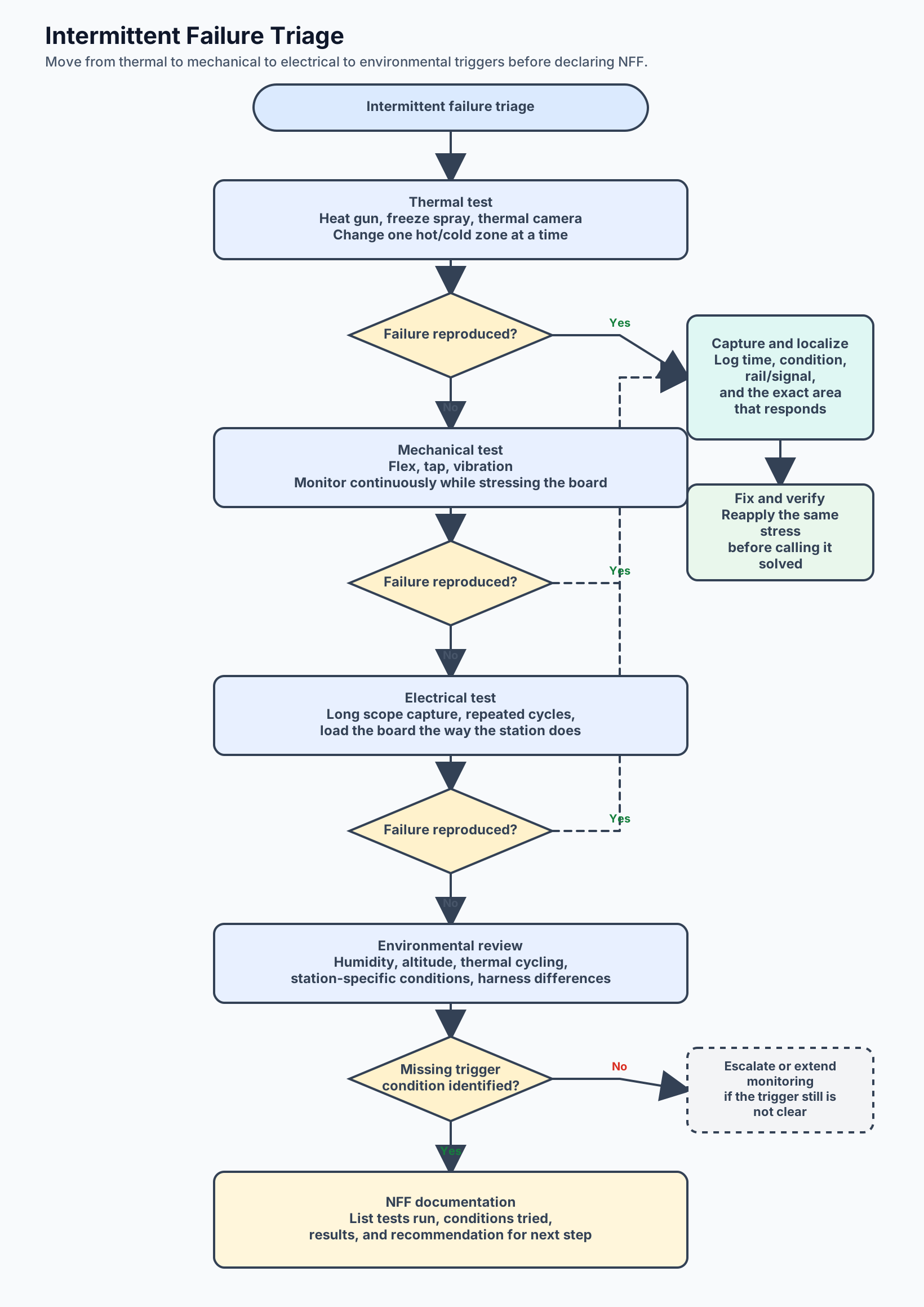
Key Takeaway
Intermittent failures don't require different tools — they require a different approach. Patience replaces speed. Controlled variable isolation replaces shotgun probing. Logging replaces memory. Reproduce the failure before you attempt the fix, and document everything whether you find it or not. The board that comes back twice with "no fault found" and no documentation is a failure of process, not a failure of skill.
Chapter 25: Power and Ground Faults
A board lands on your station. Functional test says "FAIL — no communication." You reach for the scope to check the UART lines. Stop.
Check the power rails first.
If the 3.3V rail is sitting at 1.8V because a shorted capacitor is dragging it down, nothing downstream works correctly. The UART doesn't transmit. The MCU doesn't boot. The clock doesn't oscillate. Every symptom you chase is a ghost — a consequence of the rail being wrong, not a fault in the individual circuits. You could spend an hour probing UART signals, MCU pins, and clock circuits and find "failures" at every one. None of them are the problem.
Power and ground faults are the single most important category to check first, every time.
25.1 Short to Ground
A power rail shorted to ground may cause the approved source to current-limit, a protection device to open, or a regulator to shut down. Those symptoms can also have other causes, so confirm the rail with unpowered measurements and comparison data before declaring a short.
Finding the Short
Step 1: Identify the suspect rail. Before applying power, measure resistance or diode signature from each rail to its return using the specified polarity and settling time. Modern low-voltage rails can legitimately measure only a few ohms. Compare with the schematic, design limits, or a verified board of the same revision; do not use a universal resistance threshold.
Step 2: Narrow down the location. The short could be anywhere on that rail — a shorted capacitor, a shorted IC, a solder bridge. On a dense board, dozens of components connect to the same rail.
Techniques for localizing:
- Resistance mapping. Measure resistance from the rail to ground at multiple points along the rail's distribution path. Resistance decreases as you measure closer to the short. If R = 2 ohms at the regulator output and R = 0.5 ohms at the far end of the board near a cluster of bypass caps, the short is near those caps.
- Engineering-controlled voltage injection. If an approved injection plan exists, apply only the specified node voltage, current, duration, source isolation, and sequencing controls described in Chapter 17. Use millivolt-drop mapping to follow current distribution. Never infer safe injection values from the rail's nominal operating voltage alone.
- Thermal localization. Under the same approved injection plan, use a thermal camera or other non-contact method to look for relative heating. Do not touch an energized or injected assembly; low voltage does not eliminate burn, chemical, ESD, or stored-energy hazards.
Step 3: Verify. Once you've identified the suspect component, measure it directly. Lift one end if necessary and re-measure the rail — if the short disappears, you've found it. Check the failure chain (Chapter 6) before replacing: what caused the component to short?
25.2 Open Power Rail
The opposite problem: the rail measures correct voltage at the regulator output but reads 0V at the IC it's supposed to feed. Something between them is broken.
Common Causes
- Trace breaks. A PCB trace carrying power was damaged — cracked by board flex (near a V-score line, near a mounting hole), etched too thin during manufacturing, or severed by a scratch during handling.
- Via failures. A via connecting power between layers has a cracked or insufficient barrel plating. It conducted during initial test (barely) and opened later under thermal cycling. These are invisible from the surface (see section 25.6).
- Cold joints on power components. A cold solder joint on the regulator output pin, on an inductor in a switcher circuit, on a ferrite bead in the power path, or on a power connector. The joint has enough contact for milliamp-level signals but can't carry the load current — or it's fully open.
Debug Approach
Measure voltage at the regulator output. Good? Move downstream along the power distribution path: after the ferrite bead, after the connector, at each branch point, at the IC's VCC pin. The point where voltage drops from present to absent is where the open is. Check continuity across that section. Inspect the trace, the via, the solder joint — whatever bridges that gap.
Compare to the golden board: probe the same nodes. If the golden board reads 3.31V at the MCU's VCC pin and your failed board reads 0V, but both read 3.31V at the regulator output, the break is between the regulator and the MCU.
25.3 Ground Bounce
The ground plane is not at zero volts everywhere. It's close to zero — but not exact. Current flowing through the ground path creates small voltage drops across the impedance of the ground plane, traces, and vias. This is called ground bounce, and it's a real signal integrity issue on production boards.
What It Looks Like
- Digital circuits: False triggering, corrupted data, clock jitter. The ground reference for an IC has shifted by 100-200mV due to a large return current flowing nearby. The IC's logic thresholds are now off by that amount. Usually not enough to cause a hard failure — but enough to cause marginal, intermittent errors (Chapter 24).1
- Analog circuits: Noise on the measurement. An ADC reading that bounces around or has periodic spikes synchronized with switching regulator activity. The ADC's ground reference is being modulated by the switcher's return current.
- Mixed-signal boards: A digital section's ground current couples into the analog section's ground reference. The symptom looks like analog noise but the root cause is digital.
Causes
- Insufficient decoupling capacitors — missing, cracked, or tombstoned bypass caps (Chapter 22).
- Long ground return paths — the current takes a circuitous route back to the supply because the ground plane has a split or slot that forces it around.
- High-current paths sharing ground with sensitive circuits — a motor driver's return current flowing through the same ground path as an ADC's reference.
Debug Approach
This is difficult to measure directly because you're looking for millivolt-level differences between two ground points. Use the scope: probe between two ground points on the board (not between one ground point and your scope's ground clip — that measures the difference relative to the scope ground, not relative to the board's ground). Look for AC noise synchronized with switching or digital activity.
Compare to the golden board. If the golden board shows 5mV of ground noise between two points and the failed board shows 50mV, something changed — a missing decoupling cap, a cracked ground via, a solder defect on a ground connection.
25.4 Power Rail Instability
The rail is present but not clean. The DC voltage reads correct on the DMM, but the scope reveals ripple, noise, oscillation, or transient droops.
What to Look For
- Switching ripple. Every switching regulator produces some output ripple at its switching frequency (typically 500kHz to 2MHz). Normal ripple on a well-decoupled rail is 10-30mV peak-to-peak. If you see 100-300mV, the output caps are degraded (ESR drift on electrolytics, cracked MLCCs) or the wrong type.
- Oscillation. A regulator that's unstable oscillates at a frequency unrelated to its normal switching frequency — often lower, in the 10-100kHz range. On the scope, the rail looks like it has a sawtooth or sine wave riding on top of the DC voltage. Cause: feedback loop instability from wrong output capacitor type or value (see Chapter 21, section 21.2).
- Load transient droops. The rail sits at 3.3V at idle but droops to 2.9V for several milliseconds when the MCU suddenly draws current (waking from sleep, firing up a radio, switching GPIO). If the droop is deep enough, the MCU brownouts. This points to insufficient bulk capacitance on the rail or a regulator that can't respond fast enough.
Debug Approach
Scope the rail with an AC-coupled probe to see the ripple riding on top of the DC. Use a short ground lead (spring-tip ground, not the long clip lead — the clip lead picks up noise and gives you a false reading). Compare to the golden board under the same load conditions. If the failed board's ripple is worse, check the output capacitors — value, type, ESR, and solder joint integrity.
25.5 Multiple Rail Dependencies
Modern boards have multiple power rails — 5V, 3.3V, 1.8V, 1.2V — and they often depend on each other. The 3.3V rail comes from a regulator powered by the 5V rail. The 1.8V rail comes from a regulator powered by the 3.3V rail. If the 5V rail fails, the 3.3V regulator has no input, and the 1.8V regulator has no input to its input. All three rails are down. But the failure is on the 5V rail — not on the 3.3V or 1.8V.
Power Sequencing
Some designs require rails to come up or down in a specific order, tolerate only limited pre-bias, or restrict voltage differences between domains. The order and timing are device-specific. A supervisor, PMIC, or enable chain may control them. Compare the measured sequence with the product specification and component datasheets rather than applying a generic core-before-I/O rule.
Cascade Failures
A short on the 1.8V rail overloads the 1.8V regulator, which draws excessive current from the 3.3V rail, which overloads the 3.3V regulator, which draws excessive current from the 5V rail. The thermal camera shows the 3.3V regulator overheating, so you suspect the 3.3V rail — but the root cause is the 1.8V rail short.
Debug Approach
Always start at the top of the power tree. Measure the input supply first. Then measure each rail in order of derivation: 5V, then 3.3V from 5V, then 1.8V from 3.3V. If a downstream rail is shorted, it loads the upstream rail. Finding the shorted downstream rail first (using the resistance mapping from section 25.1) prevents you from chasing a loaded upstream regulator that's actually fine.
25.6 Via Plating Defects
A via is a drilled hole connecting copper layers through the PCB stack-up. The hole is plated with copper to create the electrical connection. If the plating is insufficient, cracked, or missing, the via is an open circuit — and you can't see it from the surface.
How It Happens
- Manufacturing defect. The plating process didn't deposit enough copper in the barrel. The via passed initial electrical test (enough copper for a marginal connection) but fails later under thermal stress as the thin plating cracks.
- Thermal cycling. The PCB material (FR-4) expands in the Z-axis (through the thickness) more than the copper plating. Repeated thermal cycling — reflow, rework, operational temperature changes — stresses the barrel plating. Eventually it cracks.
- High-current vias. A via carrying more current than its plating can handle heats up, accelerating the failure. This is particularly common on power vias that should have been specified with larger drill size or multiple vias in parallel.
What the Tech Sees
An internal open on a power rail or a signal trace. The trace is intact on the surface. The component solder joints are fine. But somewhere in the middle, a via that's supposed to connect the top-layer trace to an inner-layer plane is open. Your probing from the surface shows voltage present on one side and absent on the other — but there's no visible break.
Debug Approach
When you find a voltage discontinuity between two points and the surface trace is intact, suspect a via. Probe on both sides of each via in the path. If one via has voltage on the top-side pad but not on the bottom-side pad (or vice versa), that via is open. Unfortunately, if the via connects to an inner layer that you can't probe from either surface, you may need to infer the failure from the discontinuity pattern.
There's no field fix for a failed internal via. The board needs rework routing (a jumper wire connecting the two sides of the failed via) or it needs to be scrapped. Document the location and escalate — this is a PCB fabrication quality issue.
25.7 Start With Unpowered and Power-Tree Checks
This is the summary procedure. Tape it to your station.
POWER DEBUG PROCEDURE
=====================

1. MEASURE resistance from each rail to ground
   (board unpowered)
   - Compare to golden board
   - Any rail near 0 ohms = SHORT → go to 25.1

2. APPLY power only through the authorized setup
   - Use the documented source, sequence, and protection settings
   - Capture voltage and current during startup
   - Compare under identical conditions to controlled limits or a golden board
   - If behavior leaves the authorized envelope, stop and investigate

3. MEASURE each rail voltage (DC)
   - Start from input, work downstream
   - Compare each to golden board
   - Missing voltage = OPEN → go to 25.2
   - Wrong voltage = regulator fault or loading

4. SCOPE each rail (AC-coupled, short ground lead)
   - Look for ripple, oscillation, transients
   - Compare to golden board
   - Excessive ripple = cap issue → go to 25.4

5. Only when ALL rails are correct:
   proceed to debug the reported failure
If you skip this and go straight to debugging the UART or the ADC or the motor driver, you risk spending an hour on a ghost. Five minutes checking power rails saves you that hour.
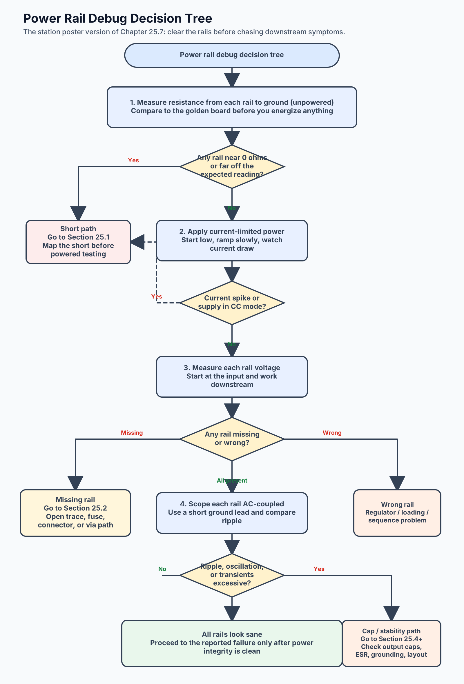
Key Takeaway
Power rails are the foundation. If they are wrong - shorted, open, noisy, unstable, or incorrectly sequenced - downstream behavior cannot be interpreted reliably. Begin with documentation and unpowered power-tree checks, then use the authorized powered setup when needed. Treat rail injection and sequencing as design-specific tests, not generic bench recipes.
Sources and notes
- Texas Instruments, "AN-643 EMI/RFI Board Design," accessed 2026-04-23, https://www.ti.com/lit/pdf/snla016; Analog Devices, "Ask the Applications Engineer-12: Grounding (Again)," accessed 2026-04-23, https://www.analog.com/en/resources/analog-dialogue/articles/grounding-again.html. The millivolt range here is an illustrative troubleshooting threshold; verify actual noise margin and ground-reference limits against the logic family, ADC/front-end, layout, and product test specification.
Chapter 26: Design and Assembly Mismatches
The board isn't broken. It was built wrong.
No cracked component. No solder defect. No thermal damage. Every joint is shiny, every part is seated, the reflow profile was textbook. And the board still fails — because the wrong component is in the right place, the right component is in the wrong orientation, or the BOM the line used was a revision behind.
Design and assembly mismatches account for a significant portion of production failures, especially during new product introduction (NPI) runs and after engineering change orders (ECOs). As a debug tech, you need to distinguish between "this board broke" and "this board was built incorrectly" — because the fix path is completely different. One goes to rework. The other goes back to process engineering.
26.1 Wrong BOM Revision
The customer updated the BOM two weeks ago. Changed R47 from 10k to 4.7k to fix a gain issue found during design validation. The ECO was issued. The new BOM was uploaded to the MES system. But the production build that ran Tuesday used a work order created three weeks ago — before the ECO — and the old BOM was loaded into the pick-and-place program.
Every board from Tuesday's build has a 10k resistor where a 4.7k should be.
What the Tech Sees
The boards fail functional test consistently. Not intermittently, not randomly — every single board from the same build lot fails the same test step. The component measures perfectly to the value printed on the schematic revision that the tech has at the station — which is the old revision. The failure only becomes apparent when someone compares the installed component to the current BOM revision and finds the discrepancy.
What to Do
- Check the BOM revision on your documentation against the BOM revision on the traveler. If they don't match, you've found the disconnect.
- If the entire lot is affected, this isn't a board-level rework. This is a production-level issue. Escalate to production engineering and quality. They need to disposition the entire lot: rework all boards, scrap, or get customer concession.
- Log it. This is a process failure, not a component failure. Your documentation should clearly state: "Board built to BOM rev B, current BOM is rev C. R47 value mismatch per ECO dated [date]."
The tech doesn't decide whether to rework the lot or scrap it. The tech finds the mismatch, documents it, and hands it off. But finding it — that's the critical step. A BOM mismatch that isn't caught at debug ships to the customer and comes back as a field failure, which costs ten times more to fix.
26.2 Pick-and-Place Errors
The placement machine puts components onto the board. It's fast and accurate — but not perfect.
Wrong Component in Right Location
The feeder for the 10k 0402 resistor ran out. The operator reloaded the feeder — but grabbed a reel of 100k 0402 resistors from the adjacent bin. Same package size, same tape width, same pitch. The machine doesn't know the difference. Every board placed after the reload has a 100k resistor where a 10k belongs.
This is extremely common with passives in small packages where the only difference between values is the marking code — and 0402 and smaller parts often have no marking at all.
Right Component, Wrong Orientation
The pick-and-place nozzle picks up the part and rotates it to the programmed angle. If the programming angle is wrong (a 90-degree or 180-degree error in the placement file), or if the nozzle mishandles the part, the component is placed rotated.
For passives without polarity (standard resistors, non-polarized capacitors), this doesn't matter. For polarized components — tantalum caps, diodes, transistors, ICs — wrong orientation means wrong electrical behavior. A reversed tantalum cap gets reverse-biased and can fail catastrophically (see Chapter 23). A rotated SOT-23 transistor has its pins swapped — collector where emitter should be, or base where collector should be.
What to Do
Compare the installed component to the BOM and schematic. For suspected wrong values, desolder and measure out of circuit. For wrong orientation, check the component marking against the schematic's pin assignment and the board's silkscreen orientation indicator.
If the error is consistent across multiple boards, it's a systematic placement issue — escalate to the SMT line. A one-off is likely a nozzle error or a single misplaced part from feeder transition.
26.3 Missing Components
Empty pads. No component installed. The placement machine skipped the location.
Causes
- Feeder issue. The component tape jammed, ran out, or the feeder was misaligned. The nozzle tried to pick and got nothing. Some machines flag this; some don't.
- Pick failure. The nozzle picked the part but dropped it in transit due to vacuum loss, nozzle contamination, or a part that's slightly out of spec dimensionally.
- Programming omission. The location wasn't in the placement program. If the BOM changed and a new component was added, but the placement program wasn't updated, the machine doesn't know to place it.
What the Tech Sees
Visual inspection catches this immediately — empty pads with solder paste reflowed but no component. The paste melted, flowed, and solidified as bare solder pads.
Electrically, a missing component is an open circuit. If it's a decoupling cap, the MCU has less power supply filtering. If it's a pull-up resistor, the I2C bus can't pull high. If it's a feedback resistor, the regulator has no feedback — output goes to the rail or to zero depending on the topology.
What to Do
Verify the location should have a component by checking the BOM and assembly drawing. Install the correct component per the BOM. Retest.
If multiple boards are missing the same component, escalate — the feeder needs to be checked, and the boards that shipped without that component need to be recalled or verified.
26.4 Reversed or Rotated ICs
Pin 1 of the IC is in the wrong corner. The IC is rotated 90 or 180 degrees from its correct orientation.
How It Happens
- 180-degree rotation. An SOIC-8 IC placed upside-down relative to pin 1. Power and ground are swapped. The IC is destroyed immediately upon power-up — or worse, it partially works but with incorrect I/O mapping, creating confusing test failures.
- 90-degree rotation. On a square QFP or QFN package, a 90-degree rotation puts every pin on the wrong pad. An STM32F103 in LQFP-48 rotated 90 degrees has VDD pins connected to GPIO pads, GPIO pins connected to ground, and ground pins connected to VDD. The result on power-up: nothing works, current draw is wildly wrong, and you may have a dead IC.
- Rotated passives with polarity. Electrolytic capacitors, tantalum capacitors, and LEDs have polarity. A reversed tantalum can short and catch fire. A reversed LED simply doesn't light — no damage, but a failed function.
Identification
Check pin 1 marking on the IC (dot, chamfer, or stripe) against the board's pin 1 indicator (dot on silkscreen, asymmetric pad shape, or assembly drawing). On QFN packages, pin 1 is often indicated by a dot on the exposed pad or a chamfered corner — both visible only under magnification.
For small packages like SOT-23, SOT-223, and SC-70, check the part orientation against the assembly drawing. These packages are easy to rotate because they're small enough that the silkscreen indicator is barely visible.
What to Do
If the IC is rotated and was powered, assume it's damaged. Remove it, install a new one in the correct orientation, and retest. Check the failure chain (Chapter 6) — a reversed IC may have sent supply voltage into an output pin of an adjacent IC, damaging it.
If multiple boards have the same rotation error, the placement program has a wrong rotation angle. Escalate to SMT engineering.
26.5 Stencil and Paste Issues
The solder paste stencil is the interface between the paste and the board. Every aperture in the stencil corresponds to a pad on the board. Get the stencil wrong and the paste deposits are wrong — and every board through that stencil inherits the problem.
Too Much Paste
Apertures that are too large or a stencil that's too thick deposits excess paste. Excess paste causes solder bridges (Chapter 22) after reflow, especially on fine-pitch components. If you're seeing consistent bridging on the same pins across multiple boards, the stencil aperture for that pad group is oversized or the stencil thickness is wrong.
Too Little Paste
Apertures that are clogged, worn, or undersized deposit insufficient paste. Insufficient paste causes weak joints, voids, or completely open connections after reflow. If a specific location consistently has insufficient solder across multiple boards, the stencil aperture is clogged or damaged.
Misaligned Stencil
The stencil isn't registered correctly to the board. Every paste deposit is shifted — left, right, up, or down — relative to the pads. After placement and reflow, components are offset. Leads or balls that should be centered on pads are hanging off the edge. This causes bridges on one side (where the solder flows between shifted pads) and opens on the other (where the solder can't reach the shifted pad).
What the Tech Sees
Stencil issues produce consistent, repeating defect patterns across every board in the lot. If board after board after board has bridges at the same IC and open joints at the same passives, it's not random — it's the stencil. Document the pattern and escalate to SMT process engineering. This isn't a board-level fix; it's a process-level fix.
26.6 Reflow Profile Mismatches
The reflow oven runs a thermal profile — preheat, soak, reflow peak, cool-down — calibrated for the specific board assembly. Different board sizes, copper weights, component densities, and component thermal masses require different profiles. The wrong profile for the board means some areas of the board get the right temperature and some don't.
Common Mismatches
- Peak too low. Solder doesn't fully melt in thermally massive areas (near large ground planes, under heavy connectors). Cold joints in those areas. Passes in the areas that reached temperature.
- Peak too high. Components exceed their maximum reflow temperature rating. Plastics deform. Crystals crack internally. Electrolytic cap seals weaken. The board looks fine but components are thermally damaged.
- Soak too short. Flux doesn't fully activate. Wetting is poor. Grainy, dull joints that are mechanically weak.
- Cool-down too fast. Thermal shock. Ceramic components (MLCCs) crack from rapid temperature change. These cracks may not be visible and may not cause immediate failure — they're latent defects that show up later as intermittent opens or shorts (Chapter 23, Chapter 24).
What the Tech Sees
Profile mismatches produce patterns: cold joints concentrated in the same thermal-mass areas across multiple boards, or a wave of cracked-MLCC failures on boards from the same production run. One board with a cold joint is a solder defect. Ten boards with cold joints in the same area — that's a profile issue.
What to Do
Log the pattern. Note which areas of the board are affected and what the defect type is. Escalate to process engineering. They need to review and re-profile the oven for this board assembly.
26.7 Distinguishing Assembly Errors from Design Issues
This is the judgment call that separates a debug tech from a parts swapper.
Assembly error: The board was supposed to be built a certain way and wasn't. The BOM says 4.7k and the board has 10k. The IC is rotated. A component is missing. The fix is rework to bring the board into conformance with the design.
Design issue: The board was built exactly as designed — and the design is wrong. The 4.7k resistor specified in the BOM is the wrong value for the circuit. The decoupling capacitor is too small. The trace is too thin for the current. The thermal relief is inadequate. The board is correctly assembled but functionally broken.
How to Tell the Difference
- Does the golden board have the same "defect"? If the golden board also has a 10k resistor at R47 and the golden board works, the 10k isn't the problem. If the golden board has a 4.7k and the failed board has a 10k, it's an assembly error.
- Does the BOM match the installed component? If the installed component matches the BOM and the board fails, the BOM might be wrong — that's a design issue.
- Does the failure affect every unit or just some? A design issue affects 100% of units (or at least all units under specific conditions). An assembly error affects the specific units that were misbuilt.
- Does the board work after rework to match the BOM? If you correct the assembly to match the documentation and the board still fails, the documentation might be wrong.
The Tech's Role
You don't redesign the circuit. You don't decide that the BOM is wrong. You identify whether the board matches its documentation, report discrepancies, and escalate design concerns with evidence.
The right escalation looks like this: "Board fails output voltage test. R47 measures 10k, BOM rev C specifies 4.7k. Replaced with 4.7k, board passes. All boards from lot 2026-0342 need to be checked — may have systematic BOM mismatch."
Or: "Board fails output voltage test. R47 measures 4.7k, matches BOM rev C. Golden board also has 4.7k and also measures same output voltage — golden board passes test with 4.82V, spec is 4.75-5.25V. Failed board outputs 4.12V. R47 is correct per BOM. Suspecting regulator or feedback network issue. Escalating to engineering."
Both of those are useful. Both give the next person in the chain what they need to act.
Key Takeaway
Not every failure is a broken component or a bad solder joint. Some boards were simply built wrong — wrong part, wrong orientation, wrong revision, wrong paste, wrong profile. The debug tech's responsibility is to identify whether the board matches its documentation, fix what can be reworked at the station, and escalate what can't. Recognizing assembly errors early prevents the same mistake from shipping on every board in the lot.
Chapter 27: How Troubleshooting Fits Into Production Flow
A board lands on your debug station. It didn't teleport there. It traveled through a sequence of machines and test stations, each one designed to catch specific kinds of defects, each one generating data about what it found — and what it didn't. Understanding that sequence isn't background information. It's directly useful. The upstream test data tells you what's already been ruled out, what's been flagged, and where the gaps are. If you don't know what the AOI checked, you'll waste time re-inspecting things that a $200,000 camera already verified.
This chapter maps the production flow from bare PCB to your bench. Know what feeds you, and you'll start every debug session with a head start.
27.1 — The Production Test Sequence
A typical SMT production line follows this sequence:
Bare PCB
    |
    v
Solder Paste Print (stencil)
    |
    v
Solder Paste Inspection (SPI)
    |
    v
Pick and Place (component mounting)
    |
    v
Reflow Oven
    |
    v
Automated Optical Inspection (AOI)
    |
    v
In-Circuit Test (ICT) or Flying Probe
    |
    v
Functional Test (FCT)
    |
    v
  PASS ──────> Ship
    |
   FAIL
    |
    v
Debug Station (you)
Every station upstream of you is a filter. SPI catches paste problems before reflow. AOI catches placement and solder problems after reflow. ICT catches electrical opens, shorts, and wrong values. Functional test catches system-level behavior. Your station catches whatever made it through all those filters.
That means the failures that reach you are either too subtle for the automated equipment, too complex for a single test to isolate, or caused by something the test coverage doesn't address. You're the last line.
27.2 — What Each Test Stage Catches and What It Misses
No test stage catches everything. Each one has blind spots, and those blind spots define what lands on your bench.
| Test Stage | What It Catches | What It Misses |
|---|---|---|
| SPI (Solder Paste Inspection) | Insufficient paste, excess paste, bridged paste, offset paste deposits | Nothing about component placement — paste only. And it's before reflow, so it can't see the final joint. |
| AOI (Automated Optical Inspection) | Missing components, tombstones, solder bridges, misaligned parts, wrong polarity (if visually distinguishable) | Anything hidden under a component body. BGA solder joints. Correct value vs wrong value if the packages look identical. Intermittent connections that look fine optically. |
| ICT / Flying Probe | Opens, shorts, wrong component values, missing components, reversed diodes — measured electrically at the pin level | System-level behavior. Timing. Firmware. Anything that requires the board to be powered and running. Also limited by fixture access — if there's no test point, it can't test it. |
| Functional Test (FCT) | System-level operation: does the board do what it's supposed to do? Power rails, communication, I/O behavior, firmware execution. | Root cause. FCT tells you the board failed step 47. It doesn't tell you why. That's your job. |
The takeaway: if a board passes AOI and fails ICT, the defect is electrically real but visually invisible — think cracked solder joints under component bodies, internal trace opens, or wrong-value parts in identical packages. If a board passes ICT and fails FCT, the individual components and connections are fine but the system behavior is wrong — think firmware, timing, analog margin, or something ICT doesn't cover.
Use this to narrow your starting point before you pick up a probe.
27.3 — Reading AOI Reports
AOI systems use cameras and algorithms to compare the board's appearance against a programmed model. When something doesn't match, the system flags it.
A typical AOI report gives you:
- Reference designator of the flagged component (e.g., C147, U23)
- Defect classification: missing, shifted, tombstone, bridge, insufficient solder, excess solder, polarity
- Image capture: the camera's photo of the flagged area, often with the expected image alongside
Here's what to know:
AOI has a false call rate. Depending on the program quality and component mix, AOI might flag 5-15% of boards, and a significant portion of those are false calls — the board is fine, but the camera algorithm saw a shadow, a reflective angle, or a component that was slightly off-center but still within spec. Operators at the AOI station review the flagged images and disposition them as real defects or false calls.
When a board reaches you with an AOI-flagged defect, someone upstream already looked at the image and decided it was real (or it was auto-failed). Check the AOI report to see exactly what was flagged and where. If the AOI flagged a bridge on U12 pins 3-4, start there. Don't re-inspect the entire board from scratch — the machine already did that.
AOI can't see under components. QFN ground pads, BGA solder balls, shielded areas — all invisible to optical inspection. If the board passed AOI but has a connection problem, these hidden joints are prime suspects.
AOI can't distinguish identical packages with different values. A 10K resistor in an 0402 package looks identical to a 100K resistor in an 0402 package under a camera. If the wrong reel was loaded on the pick-and-place feeder, AOI won't catch it. ICT will — or you will, with a meter.
27.4 — Reading ICT/Flying Probe Results
In-circuit test (whether bed-of-nails fixture or flying probe) makes electrical contact with specific test points on the board and measures individual components and connections.
A typical ICT fail report gives you:
- Test step number and name (e.g., "Step 034: R47 resistance")
- Measured value (e.g., 47.3 ohm)
- Expected range (e.g., 44.0–50.0 ohm — PASS, or 15.2M ohm — FAIL)
- Pin/net information: which test points were probed
This is gold. The ICT report is telling you exactly which component or connection failed and what it measured. If R47 should read 47 ohm and the ICT got 15.2M ohm, R47 is open — cracked part, lifted pad, cold joint, or missing entirely.
Watch for multiple related failures. If the report shows five components all failing on the same power net, you probably don't have five bad components. You have one open connection on that net — maybe a via, a trace, or a connector pin — and all the components downstream of the break read wrong because the measurement path is broken.
Watch for marginal failures. A capacitor that measures 0.98 uF against a limit of 1.0 uF minimum is a different problem than a capacitor that measures 0.00 uF. One is marginal (tolerance stacking, fixture contact resistance, or measurement uncertainty). The other is dead. Treat them differently.
Understand fixture limitations. ICT can only measure what it can physically contact. If there's no test point on a net, that net isn't tested. See Chapter 28 for more on fixture behavior.
27.5 — Reading Functional Test Results
Functional test powers the board and exercises it as a system. It loads firmware (if needed), checks power rails, exercises I/O, runs communication protocols, and verifies that the product does what the customer requires.
FCT results look different from ICT results because they're testing behavior, not individual components:
- "3.3V rail: measured 3.31V — PASS"
- "UART loopback: FAIL — no response within 500ms timeout"
- "LED test: channel 2 FAIL — current measured 0.0 mA, expected 15-25 mA"
The challenge with FCT results is that they tell you what failed but rarely why. "UART loopback: no response" could mean the UART transceiver is dead, the crystal isn't oscillating, the MCU isn't booting, a solder bridge is pulling the TX line low, or the firmware didn't program correctly. FCT identifies the symptom. You identify the root cause.
Use FCT results to identify the affected circuit block, then apply your frameworks (Chapters 9-14) to isolate within that block. If the 3.3V rail measures 0V, you know to start at the power supply section — not the UART, not the LEDs, not the MCU. If multiple tests fail and they all depend on the same rail or the same clock, look at the common dependency first (Chapter 25).
Check for sequence dependencies. Some functional tests run sequentially. If step 5 fails, steps 6-200 might also fail — not because those circuits are broken, but because step 5 was a prerequisite. A power rail that's down at step 5 will cascade failures through every subsequent test. The test log may show thirty failures when there's only one root cause.
27.6 — Turnaround Time Expectations and Prioritizing Your Debug Queue
Boards stack up. On a busy line, your debug queue might have five boards in the morning and twenty by afternoon. You can't spend three hours on one board while nineteen others wait.
Prioritize by impact:
- Line-down failures — if the entire production line is waiting on your diagnosis because every board is failing the same test, that's your top priority. Find the common cause and feed it back upstream immediately.
- Repeating patterns — if six boards are failing the same test, solve one and you've likely solved all six. Higher return on time invested.
- Single failures — individual boards with unique failure modes. Important but lower urgency than patterns.
- Customer-specific priorities — some customers have contractual turnaround requirements. Your production lead will tell you which ones.
Use the site's escalation and queue rules. Time limits depend on unit value, line impact, contractual response time, failure severity, available WIP, and the next diagnostic step. When you reach that boundary, document what you checked and ruled out, then pause, reassign, or escalate according to the production plan. Do not turn a sample duration into a universal 45-minute rule.
Track your queue visually. Whether it's a rack with tagged boards, a spreadsheet, or the MES system — know what's waiting, how long it's been waiting, and what the priority ranking is.
27.7 — High-Mix/Low-Volume vs High-Volume: How the Debug Workload Changes
The debug station feels very different depending on what kind of CM you work in.
High-volume, low-mix (e.g., one product, thousands of boards per day): You see the same board design repeatedly. You develop deep familiarity with its failure modes. Your golden board is well-characterized. Debug becomes pattern recognition — you've seen this failure before, you know exactly where to look. The challenge is speed and volume. There's always another board in the queue.
High-mix, low-volume (e.g., fifty different products, ten boards each): You see a different board design every hour. You don't have deep familiarity with any of them. Your golden board might not exist yet. Debug requires more schematic reading, more documentation review, and more first-principles diagnosis. The challenge is breadth — you have to be good at the method, not just the product, because the product keeps changing.
Most CMs fall somewhere between these extremes. But knowing where your shop sits on the spectrum helps you calibrate:
- In high-volume, invest in thorough golden board documentation and failure mode databases. Your past experience is your biggest asset.
- In high-mix, invest in your framework skills (Part 2 of this book) and your ability to read unfamiliar schematics quickly (Chapter 9). Your method is your biggest asset.
Either way, the master flowchart (Chapter 1) applies. The process doesn't change. The product knowledge does.
Key Takeaway
The debug station is not the first stop — it's the last. Every test stage upstream of you generated data and filtered defects. Learn what each stage catches, what it misses, and how to read its output. A five-minute review of AOI, ICT, and FCT reports before you touch a probe eliminates blind alleys and puts your hands on the right part of the board from the start.
Chapter 28: Working with Test Fixtures and ATE
That ICT fail report you just read? It was generated by a machine pressing spring-loaded pins against copper pads on your board, running current through components, and comparing the results to programmed limits. If one of those spring-loaded pins is worn, bent, or contaminated, the machine reports a failure that doesn't exist. You spend thirty minutes chasing a phantom defect because the test equipment lied to you.
This happens more often than most new techs realize. Before you trust the fail data, you need to understand the equipment that produced it — how it works, what it can and can't test, and how it fails.
28.1 — Bed-of-Nails Fixtures: How They Work and How They Fail
A bed-of-nails fixture is a custom-built plate studded with hundreds of spring-loaded test probes (pogo pins). Each pin is positioned to contact a specific test point on the board. The board is pressed down onto the fixture — or the fixture rises up to meet the board — and every probe makes simultaneous contact. The test system then runs its programmed sequence: measuring resistance, capacitance, voltage, continuity, and diode characteristics across combinations of those probe points.
The fixture is built specifically for one board design. A different product requires a different fixture.
Common Failure Modes
| Fixture Problem | What Happens | What the Tech Sees |
|---|---|---|
| Worn probe tip | Spring loses tension, tip flattens or mushrooms. Contact resistance increases. | Marginal failures — values slightly outside limits. Intermittent pass/fail on the same board. |
| Bent or broken probe | Probe doesn't contact the pad at all, or contacts the wrong location. | Hard open failure on a net that visually checks out fine. |
| Contamination on probe tip | Flux residue, solder paste, or oxidation on the tip. Insulating layer prevents electrical contact. | Intermittent opens. Board passes if you run it twice (second press breaks through the contamination). |
| Misalignment | Fixture mounting pins worn, board locating features damaged, or fixture warped. Probes land off-center or miss pads entirely. | Multiple failures clustered in one area of the board. Pattern shifts as alignment shifts. |
| Wiring damage | Internal wiring in the fixture breaks from fatigue or snagging. | Consistent failure on one specific net, every board, regardless of the board's actual condition. |
The Critical Lesson
When you see a board that fails ICT but looks perfect — clean solder joints, correct components, nothing visually wrong — consider the fixture before spending an hour on the board. Ask: does this same test fail on other boards? Has this failure started appearing recently? Does the board pass on a retest? If the answer to any of these is yes, the fixture may be your problem, not the board. See Section 28.5.
28.2 — Flying Probe Testers: What They Test and Their Limitations
Flying probe testers use motorized probe arms (typically 4-8 probes) that move to specific locations on the board and make measurements one at a time, sequentially. There's no custom fixture. The probe positions are programmed in software.
Advantages over bed-of-nails:
- No fixture cost — probe positions are software-defined, so any board can be tested without building custom hardware.
- Can probe both sides of the board.
- Can reach locations that a fixed fixture can't (e.g., between tightly spaced components).
Limitations:
- Slow. Each measurement requires physical probe movement. A bed-of-nails fixture tests the whole board in seconds. A flying probe test on the same board might take 5-30 minutes.
- Limited parallel measurement. With only a few probes active at once, some tests that require simultaneous access to many points are impractical.
- No powered testing. Most flying probe testers operate unpowered — they measure passive component values and connection integrity, not circuit behavior under power. (Some newer systems offer limited powered testing, but it's not universal.)
- Probe access. The probes need physical access to pads or vias. Dense BGA areas with no exposed test points are still untestable.
For the debug tech: Flying probe data is interpreted the same way as ICT data — measured value vs expected, pass or fail. The same cautions apply about probe contact reliability, though flying probes are less prone to wear patterns since the probe tips are replaced on a scheduled basis and there's no alignment fixture to drift.
28.3 — Functional Test Fixtures: Custom Test Jigs
Functional test (FCT) fixtures are different from ICT fixtures. Instead of testing individual components, they power the board and exercise it as a system.
A typical FCT fixture includes:
- Power connections — supplying the board's operating voltage(s) through edge connectors, pogo pins, or cable harnesses.
- Signal connections — connecting to communication ports (USB, UART, Ethernet, CAN), I/O pins, and sensor inputs.
- Load simulation — resistive loads, motor simulators, or other hardware that mimics what the board will drive in the final product.
- Software — a test script running on a PC or embedded controller that sends commands, reads responses, and compares results to pass/fail criteria.
FCT fixtures are often built in-house or by specialized fixture vendors. Quality varies. Some are beautifully engineered with labeled cables and documented schematics. Others are a rat's nest of hand-soldered wires on a plywood base. Either way, you need to understand what the fixture connects to and how, because when a board fails FCT, the fixture is part of the measurement loop.
Cable harnesses degrade. Repeated insertion and removal wears connector pins. Cables fatigue at stress points. A harness that's been in service for two years might have intermittent connections that cause phantom test failures.
Test software has bugs. The test sequence was written by a test engineer, possibly months or years ago, possibly under time pressure. Timing assumptions, threshold values, or sequence logic can have errors that surface only under specific conditions. If a board consistently fails one specific step but passes everything else and the circuit checks out, consider the test itself as a variable.
28.4 — Interpreting ATE Fail Logs
Automated test equipment (ATE) — whether ICT, flying probe, or FCT — generates fail logs. These logs are your primary input from the test floor. Reading them effectively saves you enormous time.
What to extract from an ATE fail log:
- The failing test step. Not just the step number — the step name and description. "Step 034: R47 resistance" is more useful than "Step 034: FAIL."
- The measured value and expected range. This tells you the magnitude of the failure. 15.2M ohm where 47 ohm is expected = hard open. 52 ohm where 44-50 ohm is expected = marginal or measurement uncertainty.
- Which nets and pins are involved. The fail log should identify the specific test points probed. Map these to the schematic.
- The sequence of failures. Multiple failures may be independent or cascaded. Five failures on the same power net = one root cause. Five failures on unrelated nets = possibly five separate issues (or one issue you haven't connected yet).
- Pass/fail history. If the MES system tracks it, check whether this board has been retested. A board that failed, was retested without any rework, and passed is a red flag for fixture or test variability — not a board defect.
Translate the machine's language into debug starting points. The machine says "U23 pin 14, measured 0.00V, expected 3.0-3.6V." You translate: the 3.3V rail at U23 is dead. Start with the 3.3V supply path, not U23 itself (Chapter 25).
28.5 — When the Fixture Is the Problem
Here's a scenario every experienced debug tech has seen: a board fails ICT, arrives at your station, and you find absolutely nothing wrong. You measure the flagged components — they're in spec. You check the solder joints — they're fine. You compare to the golden board — identical. You send it back for retest. It passes.
The fixture failed, not the board.
How to Recognize Fixture-Induced False Failures
- Intermittent pass/fail on retest. Same board, same test, different result. Boards don't spontaneously heal. The measurement changed because the contact changed.
- Cluster of failures in one board area. If five components in a 2cm x 2cm area all fail, and they're on different circuits, it's more likely that five probes in that area aren't making contact than that five unrelated components all failed simultaneously.
- Sudden yield drop. The line was running 98% first-pass yield yesterday. Today it's 85%. Nothing changed in assembly. The fixture took a hit, or probe maintenance is overdue.
- Marginal failures, not hard failures. Probe contact resistance adds to the measured value. A probe with 2 ohm of contact resistance makes a 47 ohm resistor read as 49 ohm. If the limit is 44-50, that still passes. If the limit is 44-48, it fails — and the board is fine.
What to Do
When you suspect a fixture problem:
- Retest the board. If it passes on retest, that's data.
- Test your golden board in the same fixture. If the known-good board also fails, the fixture is guilty.
- Report to test engineering. Fixture maintenance — probe replacement, alignment check, wiring audit — is not your job, but flagging the problem is. Include the data: which test steps, how many boards affected, retest results.
Don't waste hours debugging a board that the fixture convicted falsely. See Chapter 36 (Case Study — The False Failure) for a full walkthrough.
28.6 — Handling Boards in Fixtures Without Causing Damage
Test fixtures apply mechanical force. Bed-of-nails fixtures press spring-loaded probes into pads with enough pressure to break through surface oxides. Vacuum fixtures pull the board down. Clamshell fixtures close on the board from both sides.
Risks when loading or unloading boards:
- Flexing. Pressing the board into a fixture bends it. Excessive flex cracks BGA solder joints, fractures ceramic capacitors (especially large MLCCs like 22uF in 1210 packages), and stresses plated through-holes. If the fixture alignment is off, one side contacts before the other, creating a bending moment.
- Probe marks. Probes leave small dimples on test pads. That's normal. But probes that are misaligned can scrape across traces or pads, damaging solder mask or even cutting thin traces.
- Connector damage. Board-to-fixture connections through edge connectors or ZIF sockets wear with use. Forcing a board into a worn connector can bend pins — on the board or the fixture.
Your role as the debug tech: Handle boards with the same care around fixtures that you use at the debug station. Don't force a board into a fixture that feels tight. If a fixture requires excessive pressure to close, report it — something is misaligned. And when a board comes to you with suspicious marks near test points, note it. That damage may be from the fixture, not from assembly, and it may be contributing to the failure.
28.7 — Boundary Scan (JTAG) as a Test and Debug Tool
Boundary scan — formally IEEE 1149.1, commonly called JTAG — is a test method built into many ICs, especially processors, FPGAs, and complex digital devices. It lets you verify the connections between ICs without physically probing the pins.
How It Works
Chips that support boundary scan have a built-in shift register connected to every I/O pin. Through a 4- or 5-wire JTAG interface (TCK, TMS, TDI, TDO, optional TRST), you can:
- Drive a known value onto any pin of the IC.
- Read the value on any pin of the IC.
- Chain multiple ICs together — the JTAG bus daisy-chains through all boundary-scan-capable devices on the board.
This means you can check every connection between two JTAG-capable chips without touching a probe to the board. Set a logic high on pin 47 of U1, read pin 12 of U3 (which is connected to it on the schematic), and verify the connection is intact.
Why This Matters for Debug
Hidden-interconnect packages such as an Artix-7 in a BGA package have solder joints that ordinary visual inspection cannot see and conventional probes may not reach. The STM32F429 is also available in LQFP and other package families; package type must be checked from the exact part number and assembly data. Boundary scan can provide strong electrical evidence where supported, but X-ray, ICT, functional tests, interconnect test, and other methods may also be applicable. It is one tool in the coverage plan, not the only possible method.1
Common uses at the debug station:
- Verifying all connections on a BGA after rework (did the reflow reconnect everything?).
- Checking for solder bridges between adjacent pins on fine-pitch QFPs.
- Isolating which specific pin of a large IC has a connection problem when ICT reports a vague failure.
Limitations:
- Only works on ICs that support boundary scan. Passive components, analog ICs, and many simpler digital parts don't have JTAG.
- Requires a JTAG adapter and software. Your facility may or may not have this tooling at the debug station.
- Tests connections only — not component function. A chip with all connections intact can still be internally damaged.
If your debug station has JTAG capability, learn it. For BGA-heavy boards, it's indispensable.
Key Takeaway
The automated test equipment upstream of your station generates the fail data that starts your debug. Understanding how that equipment works — bed-of-nails fixtures, flying probes, functional test jigs — tells you what the data means and when to trust it. Some apparent board failures originate in the fixture, interface, test program, or measurement system. Consider those elements as variables when the evidence supports it; do not assume either the board or tester is guilty before reproducing the result.
Sources and notes
- STMicroelectronics, "STM32F427xx/STM32F429xx datasheet," package information, accessed 2026-07-18, https://www.st.com/resource/en/datasheet/stm32f429zi.pdf; IEEE 1149.1 Working Group, boundary-scan standard context, accessed 2026-04-23, https://sagroups.ieee.org/1149/1/.
Chapter 29: Quality Integration
You fixed the board. Replaced the shorted MOSFET, reflowed the cold joint on the QFN ground pad, swapped the out-of-spec capacitor. Board passes functional test. Done.
Except it's not done. The fix was the easy part. The question nobody at the debug station is asking — and somebody in the quality office desperately wants answered — is why. Why did that MOSFET short? Was it ESD? Was it a bad lot? Why was the QFN joint cold? Is the reflow profile drifting? Was it one board or twenty? Is the same failure going to show up tomorrow on the next hundred boards off the line?1
You are not just fixing boards. You are generating root cause data. Every failure you diagnose, every pattern you notice, every measurement you log feeds a quality system that exists to prevent the same failure from happening again. If you don't feed it, the system runs blind, and the same defects keep cycling through your station.
29.1 — The Tech's Role in Quality
In many CMs, the quality department and the debug station feel like separate worlds. Quality lives in offices with spreadsheets. You live on the floor with a soldering iron. But the connection between the two is direct: your debug findings are the raw material for quality analysis.
Here's how the loop works:
Production builds boards
        |
        v
Test catches failures
        |
        v
Debug station diagnoses root cause  <-- YOU ARE HERE
        |
        v
Quality analyzes patterns
        |
        v
Process engineering corrects the source
        |
        v
Production builds better boards
Your contribution is in the third box. If all you log is "replaced R47, board passed," quality has nothing to work with. If you log "R47 open — cracked 0402 resistor, mechanical stress fracture consistent with board flex during depaneling, third occurrence this week on same board design," quality has a pattern, a hypothesis, and a direction for investigation.
The difference between a tech who fixes boards and a tech who improves the line is what gets written down and how clearly it points to a cause.
29.2 — 8D Reports: What They Are and Your Contribution
8D (Eight Disciplines) is a structured problem-solving methodology used across manufacturing. When a customer complaint comes in, or when an internal quality issue is significant enough, an 8D report is opened. It walks through eight steps from team formation to permanent corrective action.
You won't fill out the entire 8D — that's typically driven by quality engineering. But you'll contribute directly to the first four disciplines:
| Discipline | What It Is | Your Role |
|---|---|---|
| D1: Team | Assemble the people who will investigate. | You may be on the team, especially for complex or recurring failures. |
| D2: Problem Description | Define the problem clearly: what, where, when, how big. | Your debug logs provide the "what" and "where." How many boards? Which test step? Which component? Which lot? |
| D3: Containment | Stop the bleeding — prevent more defective product from shipping while the investigation continues. | You identify which boards are affected. "All boards from Tuesday's build with lot code 2025-W12 on U7" gives quality the information to quarantine. |
| D4: Root Cause Analysis | Find the real cause, not just the symptom. | Your failure chain analysis (Chapter 6) is exactly this. What killed the component? Where did the condition come from? |
D5 through D8 (corrective actions, implementation, prevention, congratulations) are handled by engineering and quality. But without solid data from D2-D4, the rest of the 8D is guesswork.
Practical takeaway: When you're working a failure that looks like it might be systemic — multiple boards, same defect, same location — document it as if someone will ask you to contribute to an 8D. Because they probably will.
29.3 — 5 Whys: Tracing Back to the Process Root Cause
The 5 Whys technique is simple: keep asking "why" until you reach the root cause. In practice, it takes you from the component-level failure (your world) to the process-level cause (engineering's world).
Example:
- Why did the board fail functional test? — The 3.3V rail was at 0V.
- Why was the 3.3V rail at 0V? — The LDO regulator U14 had a solder bridge between output and ground.
- Why was there a solder bridge? — Excess solder paste on the pads.
- Why was there excess solder paste? — The stencil aperture for U14 was oversized relative to the pad geometry.
- Why was the stencil aperture oversized? — The stencil was built from an older revision of the Gerber data that used a different footprint.
You, the debug tech, found the answer to Why #1 and Why #2 — and possibly Why #3 if the bridge was visible. The stencil and Gerber investigation (#4 and #5) happens upstream, driven by process engineering. But your clear identification of "solder bridge on U14, output to ground" is what triggered the whole chain.
Without the specific, component-level root cause data from the debug station, the 5 Whys analysis never gets past "boards are failing."
29.4 — Fishbone (Ishikawa) Diagrams
A fishbone diagram organizes potential causes of a defect into categories. It's a brainstorming tool — you map out every possible contributor before investigating, so you don't fixate on the first idea.
Common manufacturing fishbone categories (the "bones") include:
- Man — operator error, training gaps, shift differences
- Machine — pick-and-place accuracy, oven profile, printer alignment
- Material — solder paste batch, component lot, PCB fabrication quality
- Method — process sequence, rework procedure, handling practice
- Measurement — test fixture accuracy, limit settings, calibration drift
- Environment — humidity, temperature, ESD, contamination2
Example: recurring tombstone defects on 0402 capacitors
Man          Machine         Material
 |              |               |
 |  Operator    | P&P placement | Paste shelf
 |  handling    | accuracy      | life expired
 |  after       |               |
 |  placement   | Oven zone     | Component
 |              | balance       | moisture
 |              |               | sensitivity
 +------+-------+------+-------+------+------+
                       |
              [Tombstone Defect]
                       |
 +------+-------+------+-------+------+------+
 |              |               |
 | Pad geometry | Fixture       | Humidity
 | asymmetry    | pressure on   | in paste
 |              | board during  | storage
 | Stencil      | reflow        | area
 | aperture     |               |
 | ratio        | Limit too     | Airflow
 |              | tight on AOI  | near oven
 |              |               |
Method       Measurement     Environment
You won't typically build the fishbone yourself — quality engineering leads that exercise. But your input populates the branches. When quality asks "could this be a material issue?" and you say "yes — I've noticed the tombstones only appear on boards using the new paste lot that arrived Monday," you've just pointed the investigation at the right bone.
29.5 — Pareto Analysis: The 80/20 of Failure Modes
Pareto analysis applies a simple observation: roughly 80% of defects come from 20% of causes. If your debug station processes 200 boards a month, a Pareto chart of failure modes will almost always show a small number of defect types dominating the list.
Example Pareto data for a month:
| Failure Mode | Count | Cumulative % |
|---|---|---|
| Solder bridge (fine-pitch QFP) | 47 | 33% |
| Cold joint (QFN ground pad) | 31 | 55% |
| Missing component (0402 passives) | 22 | 70% |
| Wrong component value | 14 | 80% |
| Cracked MLCC | 10 | 87% |
| Firmware mismatch | 7 | 92% |
| All others | 12 | 100% |
The top three failure modes account for 70% of all debug work. If process engineering fixes the solder bridging issue on fine-pitch parts and the QFN reflow profile, they eliminate more than half your workload.
Your role: Accurate, consistent failure mode classification in your debug logs. If you log "replaced U14" instead of "solder bridge on U14 pins 23-24," the Pareto analysis can't distinguish bridge defects from open defects from wrong-part defects. Specificity in logging drives specificity in analysis.
29.6 — When Your Pattern Detection Triggers a Process Investigation
Sometimes you notice recurrence before the trend is visible in a formal report. You see the same defect on the same reference designator, notice a failure-rate change after an event, or realize that affected boards share a panel position.
This is valuable. This is why experienced debug techs are worth their weight in gold to a CM.
When you spot a pattern:
- Document it immediately. Do not wait for a universal count. The reaction threshold depends on severity, product controls, expected rate, sample size, and the site's quality plan.
- Notify your lead or quality contact. A verbal heads-up plus a written summary: "Seeing repeated open on R112 (4.7K 0402) on boards from Line 1 today. Three boards so far. All from the same panel position (position 3). Possible pick-and-place feeder issue."
- Keep logging each occurrence. Every additional data point strengthens the case.
You're not expected to investigate the process. You're expected to recognize the pattern and raise it with enough data for someone else to act. That handoff — clear, specific, reference-designator-level — is what makes the quality loop close.
29.7 — Yield Metrics: DPMO, First-Pass Yield, and Debug Success Rate
Management watches numbers. Understanding what those numbers mean helps you understand why certain things get attention and others don't.
First-Pass Yield (FPY): The percentage of boards that pass all tests on the first attempt. If 950 out of 1,000 boards pass without any debug or rework, FPY is 95%. This is the headline number for a production line.
DPMO (Defects Per Million Opportunities): A normalized defect metric: defects divided by defined opportunities, multiplied by one million. The opportunity definition must be consistent and useful for the process being compared. A numeric DPMO value is not universally "good" or "bad"; interpret it against the product class, contractual target, baseline, measurement method, and reaction plan.
Debug disposition mix: Track repaired-and-passed, no-defect-found with explanation, escalated, held, and scrapped outcomes alongside cycle time and repeat returns. A single "success rate" can reward unnecessary rework or hide false-failure findings, so management should interpret it with the product and quality context.
Why this matters to you: When FPY drops, pressure increases across the line — including at your station. Understanding the metrics helps you anticipate workload changes and communicate effectively with production management. "Debug volume increased 40% this week because FPY on product X dropped from 96% to 88% after the new paste lot was introduced" is a more useful statement than "I'm buried."
Key Takeaway
Your debug work has two outputs: a repaired board and a root cause data point. The board ships today; the data point prevents failures tomorrow. Accurate, specific, reference-designator-level logging of every failure mode — not just what you replaced, but why it failed — feeds the quality system that makes the production line better. You're not just fixing boards. You're closing the loop.
Sources and notes
- The ESD example is a root-cause hypothesis, not a part-specific conclusion. For ESD mechanisms and control context, see EOS/ESD Association, "EOS/ESD Fundamentals Part 1: An Introduction to ESD," accessed 2026-04-23, https://www.esda.org/esd-overview/esd-fundamentals/part-1-an-introduction-to-esd/.
- American Society for Quality, "What is a Fishbone Diagram? Ishikawa Cause & Effect Diagram," accessed 2026-04-23, https://asq.org/quality-resources/fishbone; American Society for Quality, "What is a Pareto Chart? Analysis & Diagram," accessed 2026-04-23, https://asq.org/quality-resources/pareto.
Chapter 30: Documentation and Handoff
A board sits on the debug station. Probes are scattered. A few components are circled in marker on the solder side. The previous tech left for the day. No notes. No measurements. No log entry. Just a board mid-diagnosis with no indication of what's been tried, what's been ruled out, or what the current hypothesis was.
You're starting from zero on a board someone else already spent an hour on. Every minute they invested is gone — not because they didn't do good work, but because they didn't write it down.
This chapter is about making your debug work persist beyond the moment you do it. Documentation isn't paperwork for the sake of paperwork. It's the mechanism that turns individual fixes into institutional knowledge.
30.1 — What to Log: Everything That Matters
The rule is simple: if you measured it, write it down. If you hypothesized it, write it down. If you decided something, write down what and why.
Minimum log entries for every board that hits your station:
- Board identification. Serial number, work order, part number, revision. Whatever uniquely identifies this specific unit.
- Failure description from upstream. What the test log said. Copy the relevant fail data — step number, measured value, expected value. Don't summarize as "failed FCT." That's useless.
- Visual inspection findings. What you saw (or didn't see). "Visual inspection: no anomalies observed" is valid and useful — it tells the next person not to bother re-inspecting.
- Every measurement you take. Reference designator, test point, instrument, measured value, expected value. "3.3V rail at TP14: 0.00V, expected 3.3V." Not "rail was dead."
- Your hypothesis and the test you designed to confirm or refute it. "Hypothesis: U7 LDO not receiving input. Checked VIN at pin 1: 4.97V present. Hypothesis refuted — input is present, output is dead."
- What you did. "Removed U7 (TPS73633 in SOT-23-5). Measured output pin to ground: 0.2 ohm — internal short confirmed. Replaced with same part from stock. Post-rework measurement: 3.31V at TP14."
- Retest result. "Board retested at FCT station. PASS — all steps."
- Root cause classification. "Root cause: component failure — LDO regulator U7 internal short. No upstream cause identified; isolated failure."
- Photos. Photograph the defect before rework. Photograph the rework after completion. Timestamp them. Store them with the log entry.
That looks like a lot. In practice, it takes two to three minutes per board once you build the habit. And it saves far more time than it costs — both yours and everyone else's.
30.2 — How to Log It: Clear, Specific, Reference-Designator-Based
The difference between useful documentation and useless documentation is specificity.
Bad:
"Found bad cap near the processor. Replaced it. Board works."
Which cap? What was bad about it? Near which processor — the board has three. What did "bad" mean — shorted? Open? Wrong value? What measurement confirmed it? "Board works" — did it pass the full functional test or just power up?
Good:
"C224 (10uF 0805 MLCC, X5R, 16V) — measured 0.00uF in-circuit, expected 10uF. Located on VCORE rail feeding U12 (STM32F405RGT6). Removed and measured out-of-circuit: confirmed open. Visual inspection under microscope: hairline crack through body, consistent with mechanical stress. Replaced with same value from bin. Post-rework: C224 measures 9.8uF in-circuit. VCORE rail at TP7: 1.21V (expected 1.2V). Full FCT retest: PASS."
The second entry takes sixty seconds longer to write. But it tells the next person exactly what happened, it feeds the quality system with a specific failure mode (cracked MLCC), it identifies the potential mechanism (mechanical stress), and it leaves a measurement trail that confirms the repair was valid.
Reference designators are non-negotiable. "The cap by the processor" is ambiguous. "C224" is a unique identifier that maps to the schematic, the BOM, the layout, and every other piece of documentation about this board. Always use reference designators.
30.3 — Shift Handoffs: Continuity Across People
In a multi-shift operation, the board you started debugging at 3:45 PM will be picked up by someone else at 6:00 AM. That person has never seen this board. They don't know what you've checked, what you've measured, what you've eliminated, or what you were about to try next.
A proper handoff log includes:
- Current state of the board. "Board powered down. Probes removed. No components removed. Board in ESD bag at station 3."1
- Summary of work completed. "Verified power rails — all within spec. 3.3V, 1.8V, 5V all present and stable. Functional test failure is on UART channel 2 (no response). Probed UART TX at U8 pin 24: no signal activity during test. Clock at Y1 confirmed present — 8 MHz, clean waveform."
- Current hypothesis. "Suspect U8 (UART transceiver, MAX3232 in TSSOP-16) or connection between U8 and MCU U12. Have not yet probed U12 side of the UART traces."
- Suggested next step. "Check UART TX at U12 pin 42 to determine if signal originates from MCU. If present at U12 but absent at U8, trace path between them for open."
That handoff takes two minutes to write. It saves the next tech thirty minutes of duplicated work and the frustration of re-discovering what you already found.
If you wouldn't want to pick up a board with no notes, don't leave one that way.
30.4 — Building Your Personal Reference Library
Every measurement you log is a data point. Over time, those data points accumulate into something more valuable than any single board fix: a reference library.
Golden board data you build yourself. You measure the 3.3V rail on the ABC-1000 board at TP14 and get 3.31V. You log it. Three months later, you get another ABC-1000 at your station and the 3.3V rail reads 2.97V. You don't need the official golden board — your own logged data tells you that 2.97V is wrong because you've measured it at 3.31V before.
Known failure modes. You fix a cracked MLCC on C224 of the ABC-1000. Two weeks later, another ABC-1000 shows up with the same symptom at the same test step. You check your notes: "C224 — cracked MLCC, mechanical stress." You go straight to C224, find the same crack, and resolve it in ten minutes instead of forty.
Measurement baselines for unfamiliar boards. In a high-mix environment (Chapter 27), you see new board designs regularly. The first time you debug one, every measurement is new — you're building the baseline. The second time, you have your own reference data. By the fifth time, you know the board's personality.
Organize it. Whether it's a notebook, a spreadsheet, or notes in the MES system, structure it so you can find things. By product. By reference designator. By failure mode. The format matters less than the discipline.
30.5 — Digital vs Paper Logging
Your shop may use any of the following:
MES (Manufacturing Execution System) entries. The formal, system-of-record log. Every board disposition, root cause code, and rework action gets entered here. This is what quality reports pull from. This is what audits check. If your shop has an MES, it's mandatory — not optional, not "when I get around to it."
Traveler notes. Some shops use paper travelers that follow the board through the line. Handwritten notes in the debug section. Immediate, low-tech, no login required. The downside: handwriting is sometimes illegible, paper gets lost, and the data isn't searchable.
Station logbooks. A notebook at the debug station where techs record their work chronologically. Useful for shift-to-shift continuity and for capturing patterns that the MES might not surface ("third C224 failure this week — all same board position, all same line"). The downside: it stays at the station. Quality doesn't see it unless someone brings it to their attention.
Digital photos and scope captures. A phone camera or digital microscope captures what words can't describe. A photo of a cracked MLCC is unambiguous. A scope capture showing a missing clock signal is evidence. Store these where they're retrievable — linked to the board serial number in the MES, or in a shared folder with clear naming.
Best practice: Use whatever systems your shop requires. If the MES demands a root cause code and a disposition, enter them completely and accurately. Then supplement with whatever personal system helps you — notebook, spreadsheet, photo library. The official system feeds quality. Your personal system feeds you.
30.6 — Documentation That Didn't Happen
From the audit's perspective, if it isn't written down, it didn't happen.
This isn't philosophy. It's practical reality. When a customer asks why a specific board was shipped after rework, the answer needs to be in the system. "The tech checked it and it was fine" doesn't satisfy a quality-system audit. "Board serial 2025-03-0847, debug log shows open on R47 due to cracked solder joint, reworked with reflowed joint, post-rework measurement 47.1 ohm within spec, full FCT retest PASS on 2025-03-14 at 14:22" does.2
Scenarios where missing documentation causes real problems:
- Field return investigation. A product fails at the customer site. The RMA comes back. Quality pulls the board history and finds it was reworked at debug three months ago — but the log just says "reworked and passed." No root cause. No measurements. No photos. Was the original rework related to the field failure? Nobody knows, because nobody documented it.
- Repeat failure analysis. Quality notices that product XYZ has a 3% field return rate on a specific symptom. They pull debug records to look for patterns. Half the records say "repaired" with no failure mode detail. The data set is useless for pattern analysis.
- Regulatory audit. Medical, automotive, aerospace — industries where traceability isn't optional. An auditor asks to see the complete rework and test history for a specific serial number. If the debug station's contribution to that history is blank, the CM has a nonconformance.
None of these scenarios are hypothetical. They happen. And they're preventable with two minutes of logging per board.
The simplest rule: Every board that arrives at your station gets a log entry. Every board that leaves your station gets a log entry. What came in, what you found, what you did, what went out. Every time.
Key Takeaway
Documentation is not overhead — it's output. Every board you debug produces two deliverables: a repaired unit and a written record. The repaired unit ships once. The written record gets used by the next shift, the quality team, the customer audit, and your own future self. Two minutes of clear, specific, reference-designator-level logging per board is the highest-ROI habit a debug tech can build.
Sources and notes
- EOS/ESD Association, "ANSI/ESD S20.20-2021," accessed 2026-04-23, https://www.esda.org/store/standards/product/314/ansiesd-s20-20-2021/. Follow the site's ESD control program for packaging, labeling, and storage requirements.
- ISO, "ISO 9001:2015 - Quality management systems - Requirements," accessed 2026-04-23, https://www.iso.org/standard/62085.html. This book does not reproduce or interpret ISO 9001 requirements; the point here is that auditable quality systems depend on traceable records.
Chapter 31: Communication and Escalation
You've been staring at this board for forty-five minutes. You've checked the power rails. You've probed the clock. You've compared to the golden board. Every measurement is within spec, and the board still fails functional test step 87 — the CAN bus loopback. You've been through the signal path twice. Nothing is wrong, but something is wrong.
Here's what separates the professional from the stubborn: the professional writes down what they've checked, walks to the process engineer's desk, and says "I need another set of eyes."
Debugging is a solo activity at the bench. But it exists inside a team, a process, and an organization. Knowing when and how to communicate your findings — up, down, and sideways — is as much a part of the job as knowing how to use a scope.
31.1 — Communicating Findings Clearly
When you write a debug summary — whether it's an MES entry, an email to engineering, or a note on the traveler — the person reading it wasn't at your bench. They didn't see the board. They don't have your context. Your job is to give them enough information to understand the problem and act on it, without requiring them to repeat your work.
Structure of a clear debug summary:
- What failed. Board part number, serial number, test step, symptom. "Board ABC-1000 S/N 20250327-0412. FCT step 87: CAN bus loopback — no response. Expected ACK within 10ms."
- What you checked. List of measurements, comparisons, and tests performed. Be specific: test points, values, instruments used. "CAN_H at TP22: 2.5V DC bias, correct. CAN_L at TP23: 2.5V DC bias, correct. Differential signal during transmit: 2V peak-to-peak, matches golden board. Transceiver U19 (MCP2551 in SOIC-8) supply voltage pin 3: 4.98V, correct."
- What you ruled out. Just as important as what you found. "Ruled out: power supply to transceiver, crystal oscillator for MCU (8 MHz confirmed present and clean), solder joints on U19 (all pins continuity-tested to respective nets)."
- What you found (or didn't). "No anomaly identified at the debug station. All hardware measurements match golden board within tolerance."
- Your assessment or hypothesis. "Suspect firmware or CAN peripheral configuration issue. Board may need reflash or engineering review of CAN initialization code."
That summary gives an engineer everything they need to pick up where you left off. They're not going to re-probe the power supply — you already covered it. They'll go straight to firmware. You've saved them an hour.
What not to do: "Checked CAN bus. Couldn't find the problem. Escalating." That tells the engineer nothing. They'll re-probe everything you already probed, waste their own time, and form a low opinion of the data coming out of your station.
31.2 — Escalating Without Blame
Here's a sentence that shuts down collaboration: "Somebody on Line 2 must have loaded the wrong component."
Even if it's true, framing it as blame puts people on the defensive. The operator, the line lead, the production manager — everyone hears an accusation, and the response is defensiveness, not problem-solving.
Here's the same information, framed as data: "Boards from Line 2, lot 0327, are showing C114 measuring 100nF. BOM specifies 10nF. Checking whether a reel swap occurred on the 0402 feeder at position 14."
Same finding. No accusation. The data speaks for itself. The investigation can proceed without anyone feeling attacked.
Rules for blame-free escalation:
- Lead with measurements, not conclusions about people. "The data shows X" is always safer and more useful than "someone did Y."
- Describe what you found on the board. Not what you think someone did wrong upstream. Let the process investigation determine the cause.
- Use reference designators, values, and lot codes. Specificity removes ambiguity and keeps the conversation technical.
- If you have a hypothesis about the process cause, phrase it as a question. "Could this be related to the feeder changeover on Tuesday?" invites collaboration. "The feeder changeover on Tuesday caused this" invites argument.
This isn't about being soft. It's about being effective. Blame triggers defense. Data triggers action.
31.3 — When to Escalate
Escalation is a controlled handoff, not a fixed number of trips through a flowchart. The appropriate boundary depends on the assembly, failure severity, unit value, rework history, line impact, customer requirements, technician authorization, and evidence still available.
Escalate when:
- the next step exceeds your authorization, training, equipment, or safety controls;
- the site timebox, rework limit, reaction plan, or queue rule is reached;
- repeated tests are no longer eliminating hypotheses;
- the documentation and measured behavior contradict each other;
- the failure suggests a design, test-program, fixture, supplier, or process issue; or
- another discipline owns the evidence needed next.
Fresh eyes see things you've been looking past. A different tech might try a different starting point. An engineer might recognize a design-level issue that no amount of component probing will reveal. A test engineer might know about a known quirk of the test fixture.
Fresh eyes can help, but the reason to hand off is evidence and ownership, not an unsupported claim that a third attempt has a lower probability of success. Follow the site's defined boundary and preserve enough detail that the next person begins where you stopped.
31.4 — How to Escalate with Useful Data
An escalation without data is just passing the problem. An escalation with data is a handoff.
What to include when you escalate:
| Category | What to Provide |
|---|---|
| Board identity | Part number, serial number, revision, lot/date code |
| Failure symptom | Exact test step, measured value, expected value |
| What you checked | Every measurement, with test point locations and values |
| What you ruled out | Explicitly list the areas you've confirmed are working |
| What you suspect but can't confirm | Your current hypothesis and why you can't resolve it at your station |
| Photos and captures | Scope screenshots, thermal images, microscope photos — anything visual |
| Related boards | If you've seen the same failure on other boards, say so. Pattern data accelerates investigation. |
Package this in a format the recipient can use. If your shop uses a debug tracking form, fill it out completely. If it's an email, structure it with the categories above. If it's a verbal handoff, supplement it with a written summary.
The goal: the person who picks up this board should be able to start from where you stopped, not from scratch. Every measurement you've already taken is a measurement they don't have to repeat.
31.5 — Working with Process Engineers
Process engineers own the manufacturing process — the SMT line settings, the reflow profiles, the stencil designs, the pick-and-place programs. When your debug findings point to a process issue (solder defects, placement errors, paste problems), you'll interact with them.
What they need from you:
- Specific failure data: which components, which defect type, which boards, how many
- Lot and date information: when were the boards built? Which line? Which shift?
- Photos of the defect, especially if it's a solder quality issue
- Whether the failure is isolated or patterned across multiple boards
What you need from them:
- Context: was anything changed on the line recently? New paste lot? Stencil change? Reflow profile adjustment?
- Process data: SPI measurements, reflow profile logs, pick-and-place placement accuracy records
- Follow-up: did they find the process root cause? What changed? Should you expect the failure to stop?
The relationship works best when it's bidirectional. You give them specific floor-level observations. They give you system-level context. The combination is more powerful than either alone.
31.6 — Working with Design Engineers and OEM Customers
Occasionally your debug findings land outside the CM's process — the problem is in the design itself, or it requires the OEM customer's involvement.
Design engineers speak a different language. They think in terms of simulation models, timing margins, signal integrity analysis, and design rule checks. You think in terms of what you measured at TP14 with a Fluke 87V. Both perspectives are valid. Bridge the gap by providing your data in terms they can use: voltages, waveforms, timing measurements, scope captures.
OEM customers have different priorities. They care about their product's reliability, their ship date, and their warranty exposure. When you escalate to the customer (typically through your quality or engineering team, not directly), the data needs to be clean, professional, and definitive. "We believe the design has a marginal timing issue on the SPI bus between U12 and U23, based on these scope captures showing setup time violations under load" is actionable. "Something seems off with the SPI bus" is not.
Know your escalation path. In most CMs, the debug tech does not contact the OEM customer directly. Your findings go to your lead or engineering team, who package the communication appropriately. Follow your company's process. But make your internal report thorough enough that whoever does communicate with the customer has solid data to work with.
31.7 — Interacting with Test Operators
The test operators run the boards through ICT and FCT before failures reach you. They see hundreds of boards a day. They notice things.
Don't dismiss operator observations. "This board made a weird clicking noise when I pressed the test button" might sound vague, but it could point to a relay sticking in the test fixture, or an arcing component on the board. "The screen flickered during step 12 before it failed step 13" could indicate an intermittent power issue.
Ask operators for context when the test log is sparse:
- "Did this board fail on the first attempt, or was it retested?"
- "Were there any other boards from this panel that also failed?"
- "Did anything seem different about this one — longer test time, unusual display, different sound?"
Operators often have pattern-level awareness they don't formally report because nobody asks. A five-minute conversation at the test station can give you a starting direction that saves thirty minutes at your bench.
31.8 — Organizational Variation
Every CM structures its escalation paths differently. Some shops have a dedicated debug lead who triages and assigns boards. Some have the debug tech report directly to quality. Some have process engineers on the floor; others have them in a different building. Some CMs give technicians authority to contact the customer's engineering team. Others restrict that to management.
This book teaches the skill and the principle. Your company defines the chain.
What doesn't change regardless of org structure:
- Document before you escalate.
- Include your data — what you checked, what you measured, what you ruled out.
- Frame findings as data, not blame.
- Respect the site's escalation boundary — do not hoard a board, and do not throw it over the wall without evidence.
- Communicate clearly enough that the next person can pick up where you left off.
The organizational chart varies. The standard for professional communication doesn't.
Key Takeaway
Debugging does not end when you run out of ideas — it transitions. A well-documented escalation with specific measurements, ruled-out causes, and a clear hypothesis hands the problem to the right owner in a state where work can continue. Defined escalation criteria protect safety, WIP, and engineering time. Blame-free, data-driven communication keeps the team focused on the problem instead of on each other.
Chapter 32: Case Study — No-Boot MCU
The board is dead. No LEDs, no serial output, no response to the JTAG programmer. The functional test station logged one line: "No communication — FAIL." The operator taped a red reject sticker to the antistatic bag and dropped it in your queue.
A dead board is either the easiest or the hardest debug you'll do today. Easy, because hard failures leave obvious clues. Hard, because "no communication" could mean anything from a missing solder ball under the MCU to a blown input fuse. The test log gives you nothing to narrow it down.
This is where the flowchart earns its keep. Start at the top. Work the process. Let the board tell you what's wrong.
The Board
Industrial IoT gateway. Four-layer PCB, roughly 80mm x 60mm. The main processor is an STM32F407VGT6 in LQFP-100 — a 168 MHz Cortex-M4 with on-chip flash, running an RTOS that manages Ethernet, RS-485, and four analog input channels. Power comes in at 24V from an industrial bus connector, steps down through a TPS54331 buck converter to 5V (24V sits close to the TPS54331's 28V maximum input, so the design has limited transient margin on a 24V industrial bus), then feeds two LDO regulators: a TLV1117-33 for the 3.3V I/O rail and an XC6206P122MR for the 1.2V core rail that powers the STM32's internal PLL and analog blocks.1
The 1.2V rail is critical. Without it, the processor's core logic doesn't initialize. The chip draws power on its VDD pins (3.3V) and its VDDA pin (3.3V analog), but it also requires 1.2V on its VCAP1 and VCAP2 pins. On many STM32 designs, the 1.2V is generated internally by an on-chip regulator and the VCAP pins just need external decoupling capacitors. On this board, the designer chose an external 1.2V LDO to feed a filtered analog supply as well, with VCAP1 and VCAP2 tied to that external rail through ferrite beads.
The BOM lists 437 components. The board has been in production for eight months with a first-pass yield around 96%. This unit came off Tuesday's build and failed at functional test — first time through, no prior rework.
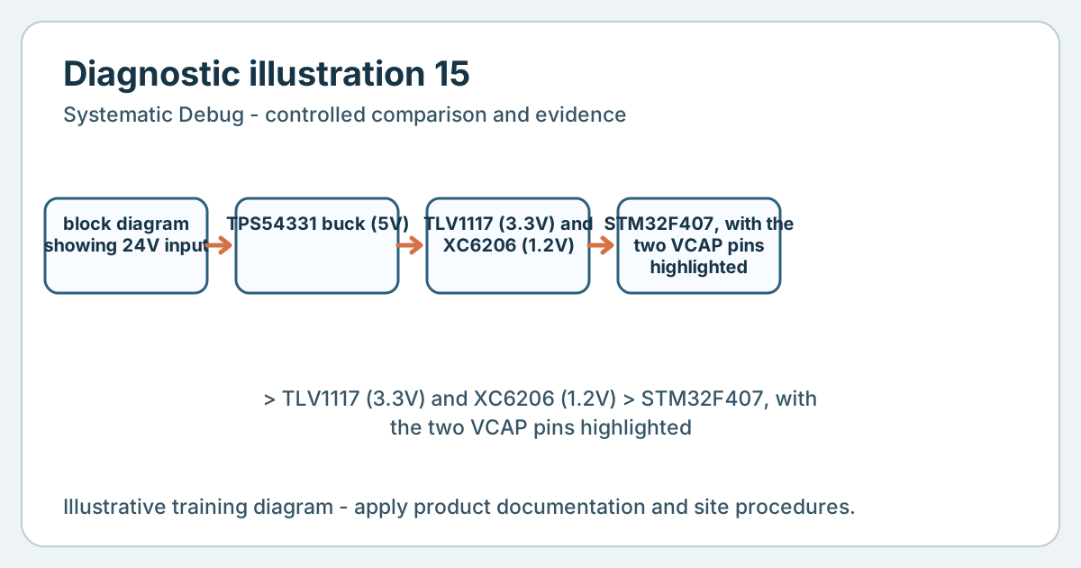
The Symptom
Functional test reports no communication. The test fixture applies 24V through the bus connector, waits for the STM32 to boot and enumerate on Ethernet, then runs a command-response sequence to verify all I/O channels. This board never enumerated. The fixture waited its full 10-second timeout and logged the failure.
That's all you get. No partial pass, no measured values, no clue about which subsystem failed. Just silence.
The Investigation
Phase 1: Read Before You Touch (Chapter 4)
The traveler says this board is on its first trip to debug. No prior rework. Built on Line 2, Tuesday second shift. Test operator notes: "Board dead — no LEDs, no Ethernet link light."
Pull up the schematic on the station monitor. Four sheets. Sheet 1: power supply. Sheet 2: STM32 and memory. Sheet 3: Ethernet PHY and magnetics. Sheet 4: analog front end and connectors. You'll need sheets 1 and 2.
Check the BOM revision against the traveler. They match. No red flags in the paperwork.
Phase 2: Sensory Inspection (Chapter 5)
Board out of the bag, onto the ESD mat. Systematic visual scan — top side, left to right, then bottom side.2
Top side: SMT components look well-placed. Solder joints on the QFP-100 MCU look clean under the stereo microscope — no bridges visible at 10x between the 0.5mm pitch pins. Buck converter area looks normal. the TLV1117-33 in SOT-223 and the XC6206 in SOT-23 appear properly soldered. Connectors seated. No discoloration, no burnt smell, no mechanical damage.
Bottom side: Ground pads on the QFN components look properly reflowed through the thermal vias. No solder balls. No bridges on the bottom-side passives.
Nothing jumps out. The board looks clean. That's data — it rules out obvious assembly damage and gross solder defects, but it means the fault is more subtle.
Phase 3: Golden Board Comparison (Chapter 7)
You grab the golden board from the ESD cabinet — same revision, verified passing last week. Set both boards on the bench side by side.2
Start with passive comparison, unpowered. Multimeter on resistance, probing the main rails to ground:
| Rail | Golden Board | Failed Board |
|---|---|---|
| 24V input to GND | 4.7 kΩ | 4.6 kΩ |
| 5V rail to GND | 890 Ω | 880 Ω |
| 3.3V rail to GND | 320 Ω | 315 Ω |
| 1.2V rail to GND | 1.2 kΩ | 0.8 Ω |
There it is. The 1.2V rail reads 0.8 ohms to ground on the failed board. On the golden board, it's 1.2 kilohms. That's not a subtle difference — that rail is dead shorted.
Phase 4: Powered Verification
Connect the current-limited bench supply to the 24V input. Set the current limit to 200mA — enough to let the buck converter start but not enough to damage anything if there's a hard short downstream.
Power up. The 5V rail comes up to 4.98V. The 3.3V rail comes up to 3.29V. The 1.2V rail sits at 0V. The XC6206 LDO is trying to regulate, but with a dead short on its output, it's dumping all its current into the short and the output voltage collapses.
Current draw on the 24V input is higher than the golden board — about 180mA vs the golden board's 120mA at idle. The excess is the LDO burning power into the short.
Confirmed: the 1.2V core rail is shorted to ground. The STM32 can't boot without its core supply. No boot, no Ethernet, no communication, test fails.
Phase 5: Isolate the Short (Chapter 10, Chapter 25)
Now the question is: what's shorting the 1.2V rail? The schematic shows the XC6206 output connects to:
- C87: 1µF 0402 MLCC decoupling cap at the LDO output
- C88: 100nF 0402 MLCC decoupling cap at the LDO output
- FB3 and FB4: two ferrite beads leading to VCAP1 and VCAP2
- C91 and C92: 2.2µF 0402 MLCCs on the far side of the ferrite beads, at the VCAP pins
- R67: a 10k feedback divider resistor (for an analog monitoring tap)
That's the full load on the 1.2V net. One of those components — or a solder defect connecting the net to ground — is the culprit.
Half-split approach: desolder FB3 to isolate the LDO output side from the VCAP side. Measure both halves.
LDO side (C87, C88, R67): still reads 0.8 Ω to ground. The short is on this side.
Under the microscope at 20x, re-examine the area around C87 and C88. These are 0402 caps sitting right next to each other on the 1.2V rail, pads about 0.3mm apart. And there — between the ground pad of C87 and the signal pad of C88 — a thin ribbon of solder connects them. It's not a massive bridge. It's a fine strand, barely visible at 10x, the kind that forms when paste volume is slightly high on tightly packed 0402s and the reflow oven's peak temperature lets it wick just far enough.
C88's pad 1 connects to the 1.2V rail. C87's pad 2 connects to ground. The bridge shorts 1.2V directly to ground.
The Fix
Rework is straightforward. Fine-tip soldering iron, 0.3mm solder wick, flux pen. Clean the bridge between C87 and C88. Inspect under the microscope to confirm complete removal — no residual solder connecting the pads.
Post-rework resistance check: 1.2V rail to ground now reads 1.15 kΩ. Close enough to the golden board's 1.2 kΩ — the small difference is within component tolerance.
Reinstall FB3 (the ferrite bead removed during isolation). Verify continuity from LDO output through FB3 to VCAP1.
Clean the rework area with IPA and a lint-free swab. Visual inspection confirms no new defects introduced.
Power up on the bench supply. The 1.2V rail comes up to 1.21V. Current draw matches the golden board. The STM32's power LED illuminates. Connect a serial console — boot messages scroll. The processor is alive.
Run the board through the full functional test fixture. All I/O channels pass. Ethernet communication passes. Analog inputs within spec. Full pass.
The Closeout
Update the traveler:
- Root cause: Solder bridge between C87 (GND pad) and C88 (1.2V pad), shorting 1.2V core rail to ground.
- Defect category: Solder defect — bridge (Chapter 22).
- Rework performed: Removed solder bridge with wick, cleaned with IPA, verified rail resistance and voltage.
- Retest result: Full pass at functional test.
Photo the rework area and attach to the digital record.
Pattern check: is this the first board with this defect, or have you seen it before on this product? Check the debug log. Two other boards from Tuesday's build also came through with 1.2V rail problems — one was a different defect (missing C91), but one had a similar bridge in the same area. Two bridges in the same tight 0402 cluster on the same build lot suggests a process issue: paste volume or stencil aperture size for that area may need review by process engineering. Flag it.
Label the board, route it to pack-out.
The Lesson
This debug took about 20 minutes. Five minutes reading documentation. Three minutes on visual inspection. Five minutes on golden board comparison — and the passive resistance check found the fault zone immediately. Five minutes isolating with half-split. Two minutes under the microscope finding the bridge. Five minutes reworking and retesting.
The critical move was the passive comparison. Measuring rail resistance to ground on both boards, unpowered, with a basic multimeter. The 1.2V rail reading 0.8 ohms instead of 1.2 kilohms was a three-order-of-magnitude red flag that pointed straight to the fault. No scope, no thermal camera, no fancy tools. Just a meter and a known-good reference.
If you'd skipped the golden board and gone straight to powered testing, you'd still have found it — the 1.2V rail at 0V would have pointed you to the LDO, and then you'd have had to figure out why the LDO wasn't regulating. But the passive comparison got you there faster and safer, without pushing current through the short.
The pattern detection at closeout matters too. One bridge is a random defect. Two bridges in the same spot on the same build lot is a process indicator. Flagging that pattern is how you prevent the next twenty boards from hitting your station with the same problem.
Concepts Demonstrated
- Chapter 4 — Read Before You Touch: Test log review, traveler check, schematic navigation to identify the power architecture before probing.
- Chapter 7 — The Golden Board: Passive resistance comparison found the shorted rail in under two minutes. Powered comparison confirmed voltage behavior.
- Chapter 10 — Half-Split: Desoldering a ferrite bead to isolate the LDO output side from the VCAP side narrowed the short to a specific board area.
- Chapter 22 — Solder Defects: Hair-thin solder bridge between tightly packed 0402 pads — a common defect on fine-pitch passive clusters.
- Chapter 25 — Power and Ground: A dead short on a core power rail killed the entire board. Power rail integrity is always the first thing to verify.
Sources and notes
- This is a fictionalized composite case study. Component names are used as concrete examples; verify production use against the current manufacturer datasheets and the actual product schematic/BOM.
- EOS/ESD Association, "ANSI/ESD S20.20-2021," accessed 2026-04-23, https://www.esda.org/store/standards/product/314/ansiesd-s20-20-2021/. Follow the site's ESD control program for benches, cabinets, bags, and handling rules.
Chapter 33: Case Study — Intermittent Power-Down
The word you dread most on a test log: intermittent.
The board passed bench testing three times. Then it went into the vibration fixture for the customer's environmental qualification screen and reset itself at the twelve-minute mark. The operator ran it again. This time it made it to twenty-two minutes before resetting. Third run: reset at eight minutes. No consistency. No repeatable trigger point. Just a board that randomly drops dead under shake and comes back to life on its own.
Intermittent failures don't hold still for your probe. They hide when you look directly at them and reappear when you turn away. You can't half-split an intermittent because the failure won't cooperate with your test schedule. You need different tools, different patience, and a different approach — one built on observation over time instead of measurement at a single instant.
The Board
Automotive telematics module. Six-layer board, 95mm x 70mm. The module pulls GPS position, cellular data, and CAN bus telemetry, packages it, and transmits over LTE to a fleet management server. Central processor is an NXP i.MX RT1062 in a BGA-196 package. Power enters at 12V from the vehicle harness, steps down through a TPS65261 triple-output buck converter providing 5V, 3.3V, and 1.8V rails. A separate TPS7A20 LDO generates a 1.0V core rail for the processor from the 1.8V bus.
The board has been in production for fourteen months. Yield is normally 98.5%. This particular unit came off Wednesday's build and passed ICT, passed bench functional test on the first attempt, then failed the vibration screening — three consecutive failures with random reset timing.
The customer's spec requires the module to survive 10G random vibration for 30 minutes without functional interruption. This board can't make it past twelve.
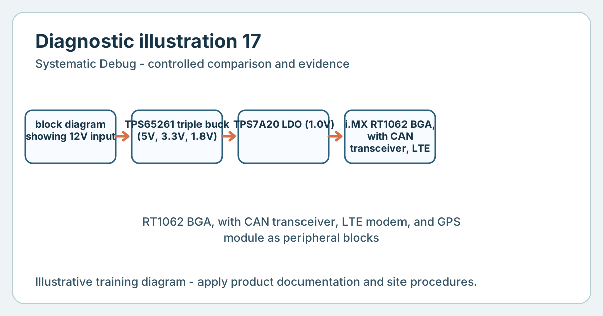
The Symptom
The functional test fixture monitors the board's heartbeat over UART during vibration screening. Every 500 milliseconds, the processor sends a status packet. When the heartbeat stops, the fixture logs a reset event with a timestamp.
Three runs, three resets at different times. No correlation to a specific vibration frequency or axis — the random vibration profile sweeps continuously. The board recovers on its own after the vibration table stops, suggesting the processor is resetting and re-booting rather than suffering permanent damage.
A reset under vibration points to one of two things: a power interruption (even a microsecond dropout can trigger the processor's brownout reset) or a broken signal connection (reset line glitching, clock dropout). The random timing and mechanical trigger make this a textbook mechanical intermittent.
The Investigation
Phase 1: Read Before You Touch (Chapter 4)
The traveler confirms: first trip to debug. Built Wednesday first shift, Line 1. Passed ICT (all opens/shorts clear). Passed bench functional (all I/O verified). Failed vibration screen three times.
The test operator added a note: "Board gets warm near U1 area during extended run — not sure if normal." That observation is worth its weight in gold. File it.
Schematic review: the TPS65261 buck converter (U4) sits on sheet 1 with its three outputs. The 1.0V LDO (U8) is on sheet 2 near the processor. The processor's brownout detection threshold is 0.88V on the 1.0V core rail — drop below that for more than a few microseconds and the hardware resets.
Phase 2: Sensory Inspection (Chapter 5)
Standard visual scan under the microscope. BGA on the processor — can't see underneath, but the perimeter balls look properly reflowed. The three buck converter inductors (4.7µH shielded, 5mm x 5mm) are cleanly soldered. The LDO in SOT-23-5 looks fine. Passives around the power section look normal. No displaced components, no cracked ceramics, no visible solder defects.
Flip the board. Bottom side clean. No solder balls, no bridging on the BGA escape vias.
Smell: nothing unusual. Touch: no loose components, no rocking on the inductors. Gentle board flex: no crackling, no audible signs of a cracked joint.
Visual inspection finds nothing. Proceed to powered testing.
Phase 3: Golden Board Comparison — Thermal (Chapter 7, Chapter 18)
Here's where the test operator's note pays off. "Board gets warm near U1 area." That's the processor. Processors get warm — that's expected. But "warm" is relative, and you have a golden board to compare against.
Power both boards on the bench. Same supply voltage, same load (both running the idle heartbeat firmware). Mount the FLIR ONE thermal camera on the bench stand, aimed at the power supply section. Let both boards soak for 30 minutes.
At 10 minutes, both boards look similar thermally. The TPS65261 on both boards runs at about 52°C — normal for a multi-output buck pushing 2W of conversion losses. The LDO on both boards reads 38°C.
At 20 minutes, something changes on the failed board. The thermal image of U4 (the buck converter) shifts. The heat signature migrates — what was centered on the IC itself now shows a hot crescent on one side, near pin 1. Temperature at that spot climbs to 61°C while the golden board's U4 holds steady at 53°C.
At 25 minutes, the hot spot is clearly asymmetric. The golden board shows even heat distribution across U4's exposed pad and package. The failed board shows the heat concentrating on the pin 1 side — the ground pad area.
Phase 4: Freeze Spray Confirmation (Chapter 24)
The thermal asymmetry suggests a high-resistance connection that's dissipating power as heat — and that resistance is changing with temperature, which explains the shifting hot spot. Time to confirm.
Board still powered, still running the heartbeat. Point the freeze spray can at U4's pin 1 corner — a short burst, maybe half a second. Watch the UART monitor.
The heartbeat stutters. The 3.3V rail, monitored on the scope, sags from 3.31V to 2.94V for about 200 milliseconds, then recovers. The 1.0V core rail dips to 0.91V — dangerously close to the 0.88V brownout threshold.
Hit it again with freeze spray. This time the heartbeat drops out entirely. The scope shows the 3.3V rail collapse to 1.7V for 400 milliseconds. The 1.0V rail hits 0.72V. The processor resets. After a few seconds, it reboots and the heartbeat resumes.
You just reproduced the intermittent on the bench. The freeze spray cools the suspect area, the solder joint's resistance increases (cracked joint — the crack opens as the metal contracts with cooling), and the rail sags enough to brown out the processor.
The golden board gets the same freeze spray treatment in the same area. No effect. Heartbeat steady, rails stable.
Phase 5: Isolate the Joint
The thermal imaging pointed to U4's ground pad area. The TPS65261 in its QFN-24 package has a large exposed thermal/ground pad on its underside — the primary path for both heat dissipation and ground current. If the solder connection between that pad and the PCB's ground plane is cracked, the ground current has to squeeze through whatever partial contact remains. That creates resistance. Resistance creates heat. Heat shifts the crack geometry. Under vibration, the crack intermittently opens and closes.
You can't see this joint. It's underneath the package. But the evidence chain is solid:
- Thermal asymmetry at the ground pad area — not present on golden board
- Freeze spray at that exact location causes the rail to sag
- Vibration causes intermittent resets — consistent with a mechanically unstable joint
- The failure is on the buck converter's ground path — the highest-current connection on the package
The Fix
This isn't a bridge you can wick away with a soldering iron. The ground pad is underneath the QFN. Proper rework requires hot air or a rework station with a component-specific nozzle.
Remove U4 with the hot air rework station. Set the bottom preheat to 150°C, top air to 260°C with the QFN-24 nozzle. Monitor with a thermocouple on an adjacent pad. The part lifts cleanly.
Inspect the exposed pad on the PCB. Under the microscope at 30x, the ground pad shows a crack pattern in the solder — a semicircular fracture running from the corner near pin 1 about two-thirds of the way across the pad. The solder surface has a dull, grainy texture along the crack line, distinct from the smooth reflowed appearance of the intact portion. This is a classic cold-side crack — likely caused by insufficient solder paste volume on the center pad during assembly, resulting in a thin joint that cracked under thermal cycling stress from the buck converter's operating heat.
Clean the pad with solder wick and flux. Apply fresh solder paste — stencil print or manual deposit to ensure adequate volume on the center pad. Place a new TPS65261 (same lot as the golden board's stock, to eliminate variables). Reflow on the rework station with the customer-specified thermal profile.
Post-rework: inspect the perimeter joints under the microscope. Clean with IPA. Measure the 3.3V rail resistance to ground — matches golden board within 5%.
Power up. All rails nominal. Run the heartbeat on the bench for 30 minutes. Hit U4 with freeze spray three times during the run. No sag, no reset, no thermal anomaly on the camera.
Send it back to the vibration fixture. Thirty minutes of 10G random vibration. Heartbeat never drops. Full pass.
The Closeout
Update the traveler:
- Root cause: Cracked solder joint on TPS65261 (U4) exposed ground pad. Insufficient solder volume on center pad created a thin joint susceptible to thermal fatigue cracking.
- Defect category: Solder defect — cracked joint / hidden joint (Chapter 22), thermally induced (Chapter 24).
- Rework performed: Removed U4, cleaned pad, re-balled and replaced with rework station, reflowed with thermal profile. Full post-rework inspection.
- Retest result: Full pass including 30-minute vibration screen.
Pattern check: query the debug log for other boards from this product with vibration failures or intermittent resets. One other board from the same build lot failed vibration two weeks ago — different tech worked it, logged "no fault found, retested pass." That board may have the same latent crack that happened to hold during retest. Flag it for re-screening.
Escalate the center pad solder volume concern to process engineering. If the stencil aperture for U4's thermal pad is undersized — or if paste transfer efficiency has degraded from stencil wear — other boards in this lot may carry the same thin joint, waiting to crack in the field under thermal cycling and vibration.
The Lesson
This debug took over an hour, and that's normal for an intermittent. The thermal camera was the key tool — not because it showed the failure directly, but because it showed an asymmetry that didn't exist on the golden board. That asymmetry was the cracked joint dissipating heat unevenly. Without the thermal comparison, you'd have been probing voltages that look fine on the bench and only fail under vibration — a much harder problem to pin down.
The freeze spray test was the confirmation step. The thermal camera said "something is wrong here." The freeze spray said "and when I stress it thermally, the rail collapses." Together, they localized the fault to a specific package and a specific connection — the hidden ground pad underneath a QFN.
The test operator's note mattered. "Gets warm near U1 area." That's sensory data from someone who handles these boards every day. They noticed something different. If you'd dismissed that note, you'd have spent more time searching. Respect the observations of the people who touch the boards before you do.
Concepts Demonstrated
- Chapter 5 — Use Your Senses: The test operator's thermal observation provided the initial lead. Visual inspection ruled out surface-level defects and directed the investigation toward hidden connections.
- Chapter 7 — The Golden Board: Thermal comparison over time revealed the asymmetric heat signature on the failed board's buck converter that didn't exist on the known-good reference.
- Chapter 18 — Thermal Imaging: The FLIR camera identified a shifting hot spot that localized the fault to a specific component and pad area — a defect invisible to visual inspection and static electrical measurement.
- Chapter 24 — Intermittent Failures: Freeze spray reproduction of the symptom on the bench, converting a random vibration-induced intermittent into a repeatable, diagnosable event. Thermal cycling fatigue as root cause mechanism.
Chapter 34: Case Study — Batch Failures from Bad Reel
Tuesday morning, the debug queue has nine boards in it. All the same product. All failed the same test — output power on the left channel. Your station normally sees two or three of these a day, spread across different failure modes. Nine boards, same failure, same day — that's not random. That's a pattern, and patterns are more valuable than any single fix.
When multiple boards fail identically, stop thinking about individual boards. Start thinking about what those boards have in common. Same build lot. Same assembly line. Same component reels. The root cause is almost certainly upstream of your station — in the materials, the process, or the test equipment. Your job shifts from "fix this board" to "find what changed."
The Board
Consumer audio amplifier. Two-layer board, 120mm x 80mm. Stereo Class-D amplifier built around two TPA3116D2 amplifier ICs (U1 for left channel, U2 for right channel) in HTSSOP-32 packages. Each channel has its own LC output filter, feedback network, and gain-setting resistors. Audio input comes through a 3.5mm jack, split into left and right paths through coupling capacitors, then through a dual op-amp (NE5532DR in SOIC-8) configured as a gain-of-2 (x2) input amplifier stage before feeding the TPA3116 inputs.
The gain on each channel is set by a resistor pair: a 20k feedback resistor from output to inverting input, and a 10k input resistor from the buffer output to the inverting input. That's a gain of 2 (6dB) — enough to drive the Class-D stage to full output power with a line-level input.
Power supply is a single 24V DC input feeding a bulk electrolytic and a ceramic bypass network. The TPA3116s run directly from 24V. The NE5532 op-amp runs from a split +/-12V rail generated by a TPS65131 dual-output boost/inverting converter, which runs from the board's 5V rail (derived from the 24V input by a small step-down regulator).
Production volume is 500 boards per week across two shifts. The product has been running for six months with 97% first-pass yield. Until this week.
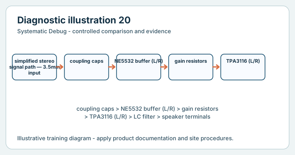
The Symptom
Functional test applies a 1kHz sine wave at 0.5V RMS to the 3.5mm input and measures output power on each channel into an 8-ohm dummy load. Pass limits: 12W to 16W per channel at 1kHz.
All nine boards fail the left channel. The right channel passes on every board — output power measured between 13.5W and 14.2W, solidly in spec. The left channel reads between 4.8W and 5.6W across the nine boards. Consistently low, but not zero. The amplifier is amplifying — just not enough.
Five-point-something watts instead of fourteen. That's roughly 4-5 dB low. Not a dead channel. Not distortion. Just low gain.
The Investigation
Phase 1: Read the Pattern (Chapter 4, Chapter 29)
Before you pick up a probe, look at what the data is already telling you.
Nine boards. Same failure. Same channel. Same test step. Same build lot — all from Tuesday second shift. Pull the production records: these boards were assembled sequentially on Line 1, serial numbers contiguous.
Right channel passes on all nine. Left channel fails on all nine, with consistent measured values (4.8W to 5.6W, tight cluster). That consistency matters — it rules out random defects. Random solder defects scatter across different channels, different failure modes, different severity. This is systematic.
What's different between the left channel and the right channel? The signal path is a mirror image — same topology, different components. Same TPA3116 part number. Same LC filter values. Same gain resistors. Same coupling caps. The only things specific to the left channel are the specific physical components loaded on the left-channel positions.
Phase 2: Sensory Inspection
Pick one board — call it Board A — and inspect. Visual scan under the microscope. Both channels look identical in solder quality. No bridges, no cold joints, no missing components on either channel. The NE5532 op-amp and its surrounding passives look clean. Both TPA3116 ICs are properly aligned and soldered.
Nothing visible distinguishes the left channel from the right. Whatever is wrong isn't a gross assembly defect.
Phase 3: Golden Board Comparison (Chapter 7)
Power up Board A and the golden board side by side. Inject the 1kHz test signal at 0.5V RMS.
Scope on the golden board's left channel: signal at U1's input pin reads 1.0V peak-to-peak — the gain-of-2 from the input network is working correctly. Output across the 8-ohm load: clean sine, 14.3W.
Scope on Board A's left channel: signal at U1's input pin reads 0.62V peak-to-peak. That's low. The signal should have been amplified by 2x (from 0.5V RMS / 0.71V peak input to ~1.0V peak-to-peak after the gain stage), but it's only reaching 0.62V. The gain is about 1.24 instead of 2.0.
The output is proportionally low — the TPA3116 is amplifying faithfully, but it's being fed a weak signal. The problem is in the gain stage, not the power amplifier.
Check the right channel on Board A for comparison: input to U2 reads 1.01V peak-to-peak. Correct. The right channel's gain stage is fine.
The fault is isolated to the left channel's gain-setting network. On the schematic, that's R7 (20k feedback) and R8 (10k input). Gain = R7/R8 = 20k/10k = 2.0. If the measured gain is 1.24, either R7 is too low or R8 is too high.
Phase 4: Component Measurement
Power down Board A. Measure R7 (feedback, marked 20k on the schematic): reads 19.8k in-circuit. That's within 1% tolerance. Fine.
Measure R8 (input, marked 10k on the schematic): reads 15.9k in-circuit.
Fifteen-point-nine kilohms. On a 10k resistor.
That's 59% high. Way outside any tolerance band. A 1% 10k resistor should read between 9.9k and 10.1k. This isn't drift — this is the wrong value.
Check the gain math: 19.8k / 15.9k = 1.245. That matches the measured gain of 1.24 exactly. R8 is the problem.
Phase 5: Confirm Across Boards
Pull R8 from Board A. Measure out of circuit: 15.8k. Not an in-circuit measurement artifact — the resistor is genuinely not 10k.
Grab Boards B through E from the failing batch. Measure R8 on each one in-circuit:
| Board | R8 Measured (in-circuit) | Expected |
|---|---|---|
| A | 15.9 kΩ | 10.0 kΩ |
| B | 15.7 kΩ | 10.0 kΩ |
| C | 16.1 kΩ | 10.0 kΩ |
| D | 15.8 kΩ | 10.0 kΩ |
| E | 15.9 kΩ | 10.0 kΩ |
All reading around 15.8k to 16.1k. Tight cluster. These are all the same wrong value.
Phase 6: Substitution Test (Chapter 13)
Pull R8 from Board A. Replace with a 10.0k 0603 1% from the debug station's parts drawer — sourced from a different reel, different lot. Retest: left channel output 14.1W. Pass.
The resistor was the problem. And it's the same wrong resistor on all the failing boards.
Phase 7: Lot Code Correlation (Chapter 8, Chapter 14)
Read the marking on the removed R8. SMD resistor code: "1582" — which decodes to 15.8k in the four-digit SMD resistor code (158 x 10^2 = 15.8k). This isn't a 10k resistor that drifted. It's a 15.8k resistor. The wrong part was loaded.
But the pick-and-place machine pulled from the feeder position assigned to R8, which should be loaded with the 10k reel. The reel label says 10k. The reel's EIA marking says 10k. But the parts on it measure 15.8k.
Check the reel's lot code and trace it through the receiving records. The reel was received from an authorized distributor three weeks ago, part number CRCW060310K0FKEA (Vishay 10k 1% 0603). Lot code: 2025-W08. This is the only reel of 10k 0603 loaded on Line 1 for the R8 position this week.
Pull five resistors from further down the same reel. Measure them: 15.8k, 15.7k, 15.9k, 15.8k, 15.8k. The entire reel is 15.8k parts in a bag labeled 10k.
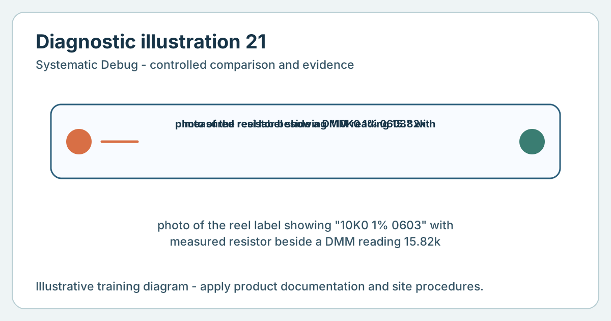
The Fix
Immediate: Replace R8 on all nine failing boards with correct 10k resistors from a verified reel. Retest each board through the full functional test. All nine pass.
Containment: How many other boards were built with this reel? Check the production records. The reel was loaded on Tuesday morning and used through end of Tuesday second shift. Total boards built with this reel in the R8 position: 47. Nine failed functional test and came to debug. The other 38 — did they pass?
Check the test data. Thirty-one of the remaining 38 boards passed functional test with left channel power readings between 12.1W and 12.8W. They passed, but barely — clustered at the low end of the 12W-16W limit. With a correct 10k resistor, these boards would have read around 14W. The wrong resistor shifted them down to marginal, and they squeaked through on tolerance stacking. Seven more boards failed with left channel readings of 5.1W to 5.9W and are still in the queue waiting for debug.
All 47 boards need R8 replaced. Notify production.
The Escalation (Chapter 31)
This goes beyond the debug station. Draft a clear escalation report:
To: Quality Engineering, Supply Chain Manager Subject: Lot code CRCW0603 2025-W08 — mislabeled reel from [distributor name]
Summary: A reel received as Vishay CRCW060310K0FKEA (10k 1% 0603) contains 15.8k resistors. The reel label, packaging, and incoming inspection paperwork all indicate 10k. Physical measurement of parts from the reel consistently reads 15.8k. Forty-seven boards affected, sixteen confirmed failing at functional test, thirty-one marginal passes requiring rework.
Evidence: Measured values from nine boards (table attached), out-of-circuit measurement of removed parts, measurement of parts pulled from the reel. Reel label photo attached. Lot code: 2025-W08.
Request: Quarantine remaining inventory of this lot code. Contact distributor for root cause (mislabeled at manufacturer? packing error at distributor?). Verify no other products in the facility use this lot code in a different position.
Escalate with data. Not with blame. "The data shows the reel contains wrong-value parts" — not "someone in receiving didn't check."
The Closeout
Update the traveler on each of the nine boards:
- Root cause: Wrong-value resistor at R8 position. 15.8k loaded in place of 10k. Source: mislabeled reel, lot code 2025-W08.
- Defect category: Component defect — wrong value from supplier (Chapter 8, Chapter 29).
- Rework performed: Replaced R8 with verified 10k 1% 0603 from alternate lot.
- Retest result: Full pass.
Log the pattern in the quality system. This is a Pareto data point — supplier-sourced material defect. It feeds the next monthly quality review and may influence incoming inspection procedures (spot-check resistor values on incoming reels, particularly from this lot period).
The Lesson
The single most important move in this debug was recognizing the pattern before picking up a probe. Nine boards, same failure, same channel, same shift — that's not coincidence, and chasing it board by board would have been nine times the work for the same answer.
The golden board comparison narrowed it in two minutes: the gain was wrong. The resistor measurement confirmed it in thirty seconds: R8 was 15.8k, not 10k. The substitution test proved it in five minutes: replace R8, board passes.
Everything after that — the lot code tracing, the reel verification, the production impact assessment, the escalation — is what separates a troubleshooter from a parts swapper. Fixing nine boards is worth 30 minutes. Catching a mislabeled reel before it builds another 200 boards is worth days of prevented rework.
The boards that passed marginally are the dangerous ones. They left the test station with "PASS" stamps, but they're running 4-5 dB low on one channel. In a consumer product, that means a customer gets an amplifier with noticeably unbalanced stereo. Returns, complaints, reputation damage. Finding those 31 boards and reworking them is just as important as fixing the nine that failed.
Trust nothing on the board (Chapter 8). Not even the reel label.
Concepts Demonstrated
- Chapter 8 — Trust Nothing: The reel label said 10k. The parts measured 15.8k. Incoming paperwork and packaging were correct on paper — the parts themselves were wrong.
- Chapter 13 — Substitution: Targeted replacement of R8 with a known-good part from a different source confirmed the diagnosis. Substitution used as confirmation, not as a starting move.
- Chapter 14 — Hypothesis-Driven: Pattern recognition (nine boards, same failure) led to the hypothesis "something common changed." Systematic narrowing identified the specific component and source.
- Chapter 29 — Quality Integration: The debug data fed directly into a quality escalation — lot code tracing, containment of 47 affected boards, incoming inspection review.
- Chapter 31 — Communication and Escalation: Clear, data-driven escalation to supply chain and quality engineering with specific evidence, lot codes, and impact assessment. No blame, just facts.
Chapter 35: Case Study — The Counterfeit Part
The readings make no sense. At room temperature, the board is perfect — every ADC channel dead-on, every calibration value within spec. Run the thermal chamber test at 50°C and channels 2 and 5 drift by 40 counts. Cool it back down, they snap to normal. Swap the board into a different test fixture — same drift at temperature. Swap a passing board into the same fixture — no drift.
The problem follows the board, not the fixture. It's temperature-dependent. And it only affects specific channels on a specific ADC. You've seen thermal intermittents before (Chapter 24), but this one has a twist: the component you'll eventually identify as the culprit looks exactly like the correct part. Same markings. Same package. Same pinout. It measures correctly at room temperature. The datasheet says it should work at 50°C.
It doesn't, because it isn't what it says it is.
The Board
Medical patient monitor, specifically the vital signs acquisition module. Six-layer board, 110mm x 85mm. The module captures ECG, SpO2, NIBP, and temperature channels through a multi-channel analog front end. Central to the design is a 16-bit, 8-channel SAR ADC — an ADS8688 from Texas Instruments in a TSSOP-38 package — sampling at 500 kSPS. Each channel has its own anti-aliasing filter, ESD protection, and signal conditioning stage. The ADC feeds a Renesas RZ/A2M processor over SPI.1
TI lists the ADS8688 as a 16-bit, 8-channel, 500-kSPS SAR ADC with an industrial -40°C to +125°C operating range, integrated analog front end, SPI-compatible interface, and TSSOP-38 package. In this fictionalized case, the customer's acceptance limit is ±4 LSB drift from the room-temperature calibration when tested at 50°C. On a 5V unipolar measurement span, one 16-bit count is about 76 microvolts, so that limit is intentionally tight.
This product has been in production for two years. Yield is historically 99.2%. In the last three weeks, five boards have failed the elevated-temperature calibration test. Before that, the failure rate on this test step was effectively zero.
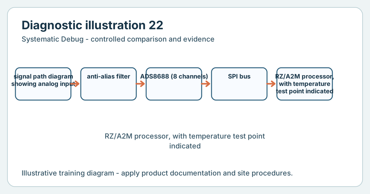
The Symptom
The calibration test runs at three temperature points: 25°C (room), 50°C, and 10°C. At each point, the test system applies precision DC reference voltages to each ADC channel and measures the digital output. The acceptance criteria compare the 50°C and 10°C readings to the 25°C baseline.
Five boards fail at 50°C. Channels 2 and 5 show drift of 30 to 45 LSB — an order of magnitude beyond the ±4 LSB limit. The other six channels on the same ADC pass on all five boards. At 10°C, those same channels drift by 8 to 12 LSB — also failing, but less severely.
The drift is always positive (reading higher than calibration). The magnitude varies between boards but the affected channels are always 2 and 5. On three of the five boards, channel 7 also shows marginal drift — 3 to 5 LSB, right at the limit.
The Investigation
Phase 1: Room Temperature Rules Out the Obvious
At 25°C, the five failing boards are indistinguishable from the golden board under the normal room-temperature test. Every ADC channel reads within the customer's room-temperature acceptance window. SPI communication is clean. Power rails are nominal. The analog front end — filters, references, conditioning stages — all produce correct voltages.
If you only tested at room temperature, these boards would pass. That's what makes this insidious.
Phase 2: Reproduce at Temperature (Chapter 18, Chapter 24)
Set up the bench thermal chamber — a small enclosure with a Peltier heater and a fan, big enough for one board. Place Board A inside, connect the SPI test harness and precision reference voltages through the chamber's cable pass-through.
Ramp to 50°C. Monitor all eight ADC channels continuously via the SPI interface, logging raw counts every second.
At 35°C, channels 2 and 5 begin drifting. By 50°C, channel 2 reads 38 LSB high, channel 5 reads 42 LSB high. The other channels hold within ±1 LSB.
Now run the golden board through the same test, same chamber, same reference voltages. At 50°C, every channel holds within ±1 LSB. Rock solid.
The problem is definitively on these boards, and it's thermal. Something about the ADC — or the signal conditioning feeding channels 2 and 5 — changes its behavior at temperature in a way the golden board's doesn't.
Phase 3: Narrow the Suspect (Chapter 14)
Hypothesis 1: The anti-aliasing filter components on channels 2 and 5 are drifting at temperature. Possible — a resistor or capacitor with a poor temperature coefficient could shift the signal.
Test: bypass the anti-alias filters by injecting the precision reference directly into the ADC's channel 2 and channel 5 input pins (after the filter). Rerun the thermal test.
Result: channels 2 and 5 still drift at 50°C. The filters aren't the cause — the error is inside the ADC itself.
Hypothesis 2: The ADC is defective — a bad silicon lot with poor thermal performance on specific channels.
Hypothesis 3: The ADC isn't a genuine ADS8688.
Phase 4: Substitution Across Sources (Chapter 13)
Desolder the ADS8688 from Board A. Replace it with one pulled from the debug station's stock — parts from a reel received six months ago, lot code ADS8688IDBT-TI-2024W31, from an authorized TI distributor.
Rerun the thermal test on Board A. All eight channels hold within ±1 LSB at 50°C. Board passes.
That confirms the original ADC was the problem. The replacement, from a different source and lot, works correctly.
Now the question: is the original ADC a genuine ADS8688 that happens to be defective, or is it something else?
Phase 5: Visual Inspection of Suspect Parts (Chapter 5, Chapter 8)
Pull the ADCs from all five failing boards. Line them up under the stereo microscope alongside three known-good ADS8688s from the authorized-source reel.
| Feature | Known-Good (authorized reel) | Suspect (failing boards) |
|---|---|---|
| Top marking, line 1 | ADS8688 | ADS8688 |
| Top marking, line 2 | IDBT | IDBT |
| Date code | 2431 (2024, week 31) | 2418, 2419, 2422, 2420, 2421 |
| Package finish | Uniform matte black | Slightly rougher, faint swirl marks |
| Lead finish | Bright, uniform tin plating | Slightly duller, minor unevenness |
| Laser mark depth | Consistent, sharp edges | Slightly shallower on two parts |
Two observations stand out.
First: the date codes. The five suspect parts carry five different date codes spanning weeks 18 through 22, while the controlled comparison reel has one. Mixed codes can have legitimate explanations, so this is not proof of fraud. Here it conflicts with the receiving and traceability records and therefore strengthens the case for quarantine and specialist review.
Second: the package finish. Two suspect parts differ from the authenticated comparison samples under the same lighting and magnification. Resurfacing is one possible cause, but normal manufacturing variation or handling could also explain it. The technician records the difference without assigning authenticity from appearance alone.
Phase 6: Preserve and Escalate
The technician stops bench experimentation. The removed parts, comparison parts, reel, labels, receiving records, and test data are segregated and preserved. No solvent, scraping, decapsulation, or other evidence-altering test is performed at the debug station. Quality opens the site's suspect-material investigation and defines the comparison and laboratory plan.
At this stage the evidence supports suspected nonconforming or counterfeit material, not a confirmed counterfeit finding.
The Escalation (Chapter 31)
This is no longer a debug-station problem. This is a supply chain integrity issue on a medical device.
Immediate actions:
- Quarantine all remaining inventory of the suspect ADC reel. Log the reel's receiving lot code, supplier, and purchase order.
- Photograph all suspect parts with comparison to authenticated parts. Document the visual differences, traceability discrepancy, and electrical test data without altering the samples.
- Notify QA management. On a medical product, this triggers a formal investigation per the company's counterfeit parts mitigation procedure (likely referencing SAE AS6171 or equivalent).
Escalation report:
To: Quality Assurance Director, Supply Chain Manager, Program Manager Subject: Suspected counterfeit ADS8688 ADCs on [product name] — five boards affected, reel quarantined
Summary: Five boards failed elevated-temperature ADC calibration. The failure followed the installed ADC, and replacement with authenticated parts from authorized stock resolved it. The removed parts also show date-code and package-finish discrepancies relative to the receiving records and comparison samples. The material is quarantined as suspect pending qualified authenticity and failure analysis.
Evidence attached:
- Thermal test data (five boards, before and after ADC replacement)
- Microscope photos (suspect vs known-good comparison)
- Chain-of-custody record for removed and comparison samples
- Reel label and lot code documentation
- Receiving records and purchase order for the suspect reel
Recommended next steps:
- Decap analysis of suspect parts to confirm die identity (coordinate with outside failure analysis lab)
- Supply chain trace: which supplier provided this reel, through what channel, with what certificates of conformance?
- Screen all inventory from this supplier for similar anomalies
- Review incoming inspection procedures for high-reliability ADCs
Phase 7: Decap Confirmation
The QA team sends two suspect parts and one known-good part to an outside failure analysis lab for decapsulation and die inspection. Two weeks later, the results come back.
The known-good ADS8688 contains a TI die with the expected geometry, bond wire pattern, and die markings consistent with the ADS8688 design.
The suspect parts contain a die and bond-wire pattern inconsistent with the authenticated ADS8688 comparison and with the external marking. Additional material and marking analysis supports resurfacing and remarking. The laboratory finding confirms that the packages are not authentic ADS8688 devices; the available evidence does not establish their exact original product or history.
At room temperature, the substituted die's behavior happened to remain inside the fictional test limits. At temperature, its drift exceeded those limits, most visibly on the higher-gain channels. This behavior is part of the fictional scenario; it is not a claim about a specific alternate TI product.
The Closeout
Update the traveler on all five boards:
- Root cause: Counterfeit ADC. Parts marked as ADS8688IDBT are re-marked lower-resolution ADC parts. Visual indicators: mixed date codes, surface refinishing marks, ink-based markings.
- Defect category: Counterfeit component (Chapter 8).2
- Rework performed: Replaced U3 (ADS8688) with verified genuine parts from authorized TI stock. Full post-rework inspection and thermal retest.
- Retest result: Full pass at 25°C, 50°C, and 10°C.
The supply chain investigation traces the reel to a broker purchase. The authorized distributor had the ADS8688 on 26-week lead time. A buyer sourced a bridge reel from a third-party broker to avoid a production line-down situation. The broker provided a certificate of conformance — which turned out to be fabricated.
Incoming inspection had checked the reel label and verified the part number against the PO. They did not perform electrical testing or detailed visual inspection of the parts themselves. The counterfeit parts looked close enough to pass a cursory check.
The corrective action is risk-based: broker purchases for this product line are suspended pending a supplier audit, purchase controls and traceability requirements are revised, and quality engineering defines qualified inspection and laboratory screening for material obtained outside authorized channels. No single visual or solvent test is treated as universal proof of authenticity.
The Lesson
This debug started with a simple thermal drift and ended with a supply chain fraud investigation. The technical diagnosis was the easy part — substitution testing and visual comparison identified the bad parts in under two hours. The larger impact was in what happened after: the quarantine, the decap analysis, the supply chain trace, the corrective action.
The clues were visible at the inspection level: traceability records did not explain the mixed date codes, and package finishes differed from authenticated comparisons. Those clues justified containment and investigation. They did not, by themselves, prove what was inside the packages.
You do not need to establish authenticity at the debug station. You need controlled comparisons, clean documentation, preserved traceability, and the discipline to stop and escalate when the evidence no longer fits ordinary failure modes. The thermal failure was the symptom; substitution isolated the suspect component; the records and visual differences justified containment; qualified laboratory analysis provided confirmation.
The five boards that failed caught the problem. The danger was the boards that might have passed with these parts at the edge of the acceptance window, shipped into a medical device, and drifted in the field when a patient's temperature readings mattered. Pattern detection and escalation aren't bureaucratic overhead. They're how you prevent that.
Concepts Demonstrated
- Chapter 5 — Use Your Senses: Visual inspection under magnification revealed surface finish anomalies, inconsistent date codes, and marking quality differences between suspect and known-good parts.
- Chapter 8 — Trust Nothing: The component markings said ADS8688. The package looked like an ADS8688. The room-temperature performance looked acceptable. The die did not match the marking. Labels lie.
- Chapter 14 — Hypothesis-Driven: Systematic elimination — bypassing the filters to isolate the ADC, then substitution to confirm, then visual inspection to explain why. Each step narrowed the hypothesis until only one explanation remained.
- Chapter 18 — Thermal Imaging: Temperature-controlled testing reproduced the failure on demand and confirmed it was specific to the suspect boards, not the test setup.
- Chapter 24 — Intermittent Failures: Temperature-dependent drift that only manifested above 35°C — invisible at room temperature, consistent at elevated temperature. Classic thermal intermittent mechanism, but caused by a fundamentally different die rather than a marginal defect.
- Chapter 31 — Communication and Escalation: Data-driven escalation with photographic evidence, test data, and supply chain traceability. The tech's detection triggered a formal counterfeit investigation that changed incoming inspection procedures.3
Sources and notes
- Texas Instruments, "ADS8688 data sheet, product information and support," accessed 2026-04-23, https://www.ti.com/product/ADS8688.
- ERAI, "Electronic Supply Chain Counterfeit Reporting and Avoidance," accessed 2026-04-23, https://www.erai.com/. This case study is fictionalized training material; real investigations should follow the company's counterfeit-control, quarantine, traceability, supplier-quality, and regulatory procedures.
- Fictionalized composite case study created for training. It is not a record of a specific employer, supplier, lot, customer, medical-device incident, or formal investigation.
Chapter 36: Case Study — The False Failure
Twelve boards sit in your queue, all stamped with the same failure: output voltage out of spec. The test log says each one measured between 3.26V and 3.28V on the main output rail. The pass window is 3.30V to 3.36V. Every board missed by 20 to 40 millivolts.
You pull the first board, power it up on your bench supply, and probe the output with your calibrated multimeter. It reads 3.33V. Dead center of the pass band.
You probe it again. 3.33V. You power cycle and re-probe. 3.33V.
The board isn't failing. So why did the test station say it was?
This is the most frustrating kind of debug: you can't fix a board that isn't broken. But twelve boards didn't fail by coincidence. Something made the test station read 3.28V when the output is actually 3.33V. And until you figure out what, every board that goes through that station is going to get the same wrong answer.
The Board
Telecom power supply module. Four-layer board, 65mm x 50mm. The module takes 48V DC from a telecom rack backplane, converts it through an isolated half-bridge LLC resonant converter to produce a regulated 3.3V output at up to 30A for downstream line cards. Output regulation is managed by a UCC25600 LLC resonant controller on the primary side, with the output sensed by a secondary-side TL431 shunt reference driving an optocoupler across the isolation barrier. Output voltage accuracy is critical — the downstream line cards have tight supply requirements.
The output is sensed at two points: a Kelvin-connected sense pair routed directly from the output terminals back to the UCC25600's feedback divider, and a separate test point pair (TP5 and TP6) routed to a pad array where the functional test fixture's bed-of-nails probes make contact.
The board has been in production for three years. Yield is historically 99.4%. Output voltage regulation has never been a significant failure mode — until this week.
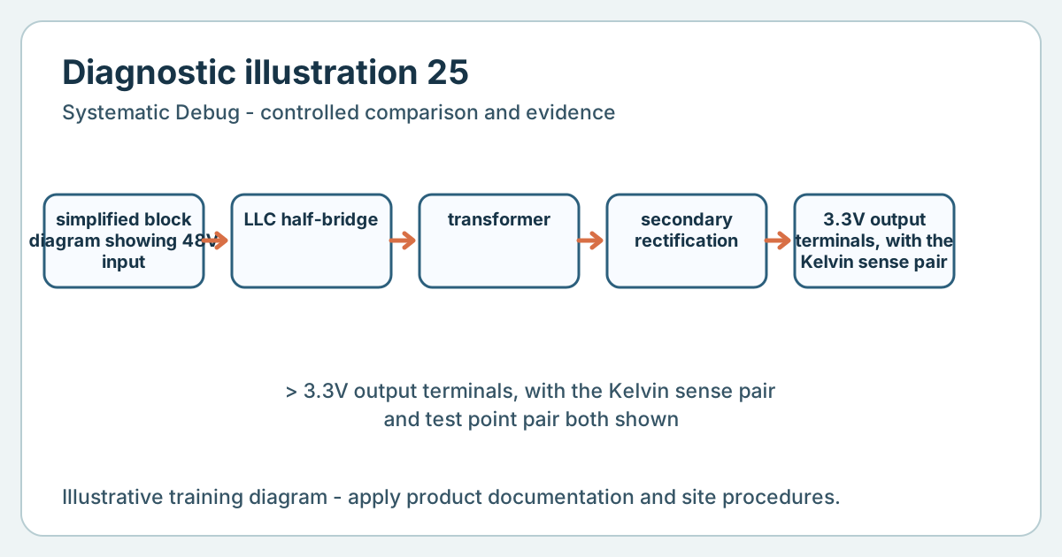
The Symptom
The functional test station applies 48V to the input, loads the output with an electronic load at 15A (50% rated load), and measures the output voltage through the bed-of-nails fixture at TP5 and TP6.
Pass limits: 3.30V to 3.36V.
Twelve boards from Thursday's production run measured between 3.26V and 3.28V. All twelve within a tight 20mV cluster, all below the lower limit by the same margin. No boards measured within the pass band. No boards measured wildly out of spec. Just a uniform downward shift.
The test operator flagged it to the line supervisor after the fifth consecutive failure. The supervisor ran two boards again — same readings. Boards pulled and sent to debug.
The Investigation
Phase 1: Read Before You Touch (Chapter 4)
Look at the numbers before you look at the boards.
Twelve boards. Same failure. Same test step. Same measurement — all clustered between 3.26V and 3.28V. Not scattered. Not random. Not some at 3.2V and others at 2.9V. A tight cluster, uniformly shifted low by about 50mV from the expected 3.33V center.
Check the production records. These boards are from Thursday first shift, Line 3. Serial numbers are not all contiguous — they span about 40 boards worth of production, meaning roughly 30% of Thursday's output from this station is failing. The other 70% passed, but pull their test data too: the passing boards measured between 3.30V and 3.32V. Also low — just barely clearing the lower limit.
Now look at the previous week's test data for the same product on the same station. Last week, output voltage readings centered around 3.33V to 3.34V with a range of 3.31V to 3.36V. This week, the entire distribution has shifted down by about 50mV.
That shift didn't happen on the boards. Boards are built from the same BOM, same components, same process. A 50mV systematic shift across all boards points to the measurement, not the product.
Phase 2: Quick Bench Verification
Pull Board A from the queue. Power it on the bench supply at 48V, electronic load at 15A. Probe the output terminals directly with the bench DMM (Keysight 34461A, calibrated last month).
TP5 to TP6 (the test point pads): 3.332V.
Output terminals directly: 3.334V.
Board A is producing 3.33V. Well within spec. The 2mV difference between the test points and the terminals is normal trace resistance at 15A.
Run Boards B and C through the same bench test. Board B: 3.331V. Board C: 3.335V. All three are fine.
The boards aren't the problem.
Phase 3: Golden Board on the Suspect Fixture (Chapter 7, Chapter 28)
This is the critical step. Take the golden board — verified passing, known 3.33V output — and run it through the same functional test fixture that failed the twelve boards. Same station, same fixture, same test program.
Result: the golden board measures 3.28V on the fixture.
The golden board, which produces 3.33V as verified by your calibrated bench DMM, reads 3.28V on the functional test fixture. The fixture is reading 50mV low. Every board going through this fixture gets the same 50mV penalty. Boards that are genuinely at 3.33V get scored as 3.28V. That puts them 20mV below the 3.30V lower limit, and they fail.
The boards that passed Thursday were genuinely at the high end of the output distribution — 3.34V to 3.36V — and the 50mV fixture error brought them down to 3.29V to 3.31V, just barely passing. The boards that failed were genuinely at the center or low-center of the distribution — 3.31V to 3.33V — and the fixture error dragged them below the limit.
The product hasn't changed. The fixture has.
Phase 4: Diagnose the Fixture (Chapter 28)
The fixture measures output voltage through a bed-of-nails probe pair contacting TP5 and TP6. Probe the fixture side of the connection — the pins in the fixture itself.
Measure resistance from the fixture's TP5 probe tip to the fixture wiring harness termination where the cable connects to the test system's DMM.
TP5 probe: 0.87 Ω. That's high. A new spring-loaded probe in good condition should measure under 0.05 Ω.
TP6 (ground reference): 0.92 Ω.
Combined: 1.79 Ω of extra resistance in the measurement path. At 15A load current, some of that load current flows through the sense path if the fixture's Kelvin connection isn't properly isolated — and on this fixture, the voltage sense and the power delivery share the same probe pins. That 1.79 Ω resistance drops voltage across the probes, and the DMM at the end of the cable reads the output voltage minus the probe drops.
Quick math: if even 30mA of bias current from the test system's DMM input flows through 1.79 Ω, that's only 54mV of drop. But the actual mechanism is simpler — the high-resistance probes create a poor contact to the test pad, and the contact resistance itself introduces measurement error. The DMM reads the voltage at the far end of a resistive connection instead of at the pad surface.
Pull the fixture's probe plate. Inspect the TP5 and TP6 probes. Both are visibly worn — the spring-loaded tips are darkened, the contact surfaces pitted from thousands of insertions against gold-plated pads. The springs feel weak compared to the adjacent probes that were replaced more recently.
Check the fixture's maintenance log. Last probe replacement: five months ago. The fixture has processed approximately 8,000 boards since then. The TP5 and TP6 probes — high-current sense probes on a power supply module — have taken more wear than the signal-level probes because the pads carry higher current and the contact interface degrades faster.
The Fix
Immediate — fixture maintenance:
Replace the TP5 and TP6 probes with new spring-loaded pins from the fixture manufacturer's spec (Everett Charles Technologies P/N ECT-025-0001 or equivalent per the fixture BOM). While the fixture is open, inspect all other probes — replace any that show visible wear, dark tips, or weak spring action. This fixture has 127 probes; six others show signs of wear and get replaced too.
Reassemble the fixture. Run the golden board through the station.
Result: 3.334V. Right where it should be.
Run Board A through the station: 3.332V. Pass.
Containment — retest the "failed" boards:
Run all twelve rejected boards through the repaired fixture. Results:
| Board | Original Reading | Retest Reading | Result |
|---|---|---|---|
| A | 3.27V | 3.332V | PASS |
| B | 3.28V | 3.331V | PASS |
| C | 3.26V | 3.335V | PASS |
| D | 3.27V | 3.329V | PASS |
| E | 3.28V | 3.334V | PASS |
| F | 3.28V | 3.330V | PASS |
| G | 3.27V | 3.336V | PASS |
| H | 3.26V | 3.332V | PASS |
| I | 3.28V | 3.331V | PASS |
| J | 3.27V | 3.333V | PASS |
| K | 3.28V | 3.335V | PASS |
| L | 3.26V | 3.330V | PASS |
All twelve pass. No rework performed on any board. Zero boards were actually defective.
Broader check: Review the past week's test data from this station. Were any boards from earlier in the week also marginally affected by probe wear? Pull the test data trend. The fixture's measurement error didn't appear suddenly — probe wear is gradual. Over the past three weeks, the station's average output voltage reading has been drifting downward: 3.33V three weeks ago, 3.32V two weeks ago, 3.31V last week, 3.28V this week. The wear was progressive.
Some boards from last week and the week before may have been marginal passes that should have been comfortable passes, or marginal fails that were retested and squeaked through. No boards were incorrectly failed and scrapped — the error only recently exceeded the tolerance margin — but the trend was there in the data, invisible because nobody was watching it.
The Escalation (Chapter 31)
To: Test Engineering, Quality Manager Subject: Fixture Station 3 — output voltage probes worn, 12 false failures, PM schedule review needed
Summary: Twelve boards from Thursday's build failed output voltage regulation test. Root cause: worn bed-of-nails probes on TP5 and TP6 introduced measurement error of approximately 50mV. All twelve boards confirmed in-spec on bench testing and pass on the repaired fixture. No boards required rework.
Data: Probe resistance (0.87 Ω and 0.92 Ω vs <0.05 Ω spec), SPC trend showing gradual measurement drift over three weeks, before/after retest data for all twelve boards.
Recommendations:
- Implement a fixture probe PM schedule based on insertion count. Suggested threshold: 5,000 insertions for high-current sense probes, 10,000 for signal-level probes.
- Add a fixture verification step to the daily startup procedure: run the golden board through each station at shift start and compare to its known values. Flag any station where the golden board reading drifts beyond a defined guard band (e.g., ±10mV for this product).
- Review SPC data for gradual measurement drift as an early indicator of fixture degradation — set control limits that trigger investigation before the drift reaches the test limit.
The Closeout
Update the travelers on all twelve boards:
- Root cause: False failure caused by worn fixture probes on test station 3. No board defect.
- Defect category: Test fixture error (Chapter 28).
- Rework performed: None. Boards are as-built.
- Retest result: All pass after fixture probe replacement.
Log the event in the quality system as a fixture-induced false failure. This data point feeds the Pareto analysis (Chapter 29) — false failures from fixture wear are a known category, and their frequency justifies the investment in a probe replacement PM schedule.
No boards scrapped. No rework time wasted. Total debug time: about 45 minutes, most of it in the fixture diagnosis and probe replacement. The twelve boards go back to production with clean test records.
The Lesson
Not one minute of soldering iron time was spent on this debug. Not one component was replaced. The boards were never the problem. Twelve units of a three-year-old, well-characterized product don't simultaneously develop the same 50mV voltage error by coincidence. The pattern — same failure, same magnitude, same station — screamed "measurement error" from the start.
The golden board was the decisive tool. Running the known-good reference through the suspect fixture proved the fixture was lying in under five minutes. Without that step, a tech might have started probing the output feedback loops, checking the optocoupler, measuring the reference divider — burning an hour per board chasing a fault that doesn't exist. Multiply that by twelve boards and you've wasted a day and a half.
The SPC trend data told the rest of the story. The fixture didn't break on Thursday. It had been degrading for three weeks — the measurement error grew from imperceptible to catastrophic as the probes wore. The boards that failed were the canary. The boards that marginally passed were the warning nobody saw.
The preventive action — a probe PM schedule and a daily golden board verification — is where this case study pays for itself. Replacing eight probes takes fifteen minutes and costs a few dollars. Diagnosing twelve false failures, retesting them, disrupting production scheduling, and stressing the debug queue costs hours and damages throughput. The PM schedule prevents the cost. The daily golden board check catches the drift before it reaches the test limit.
This is the retest path on the master flowchart (Chapter 1, Path C). The disposition wasn't "rework" or "debug." It was "retest" — because the original test was wrong. Recognizing that possibility early, and having the discipline to verify the test system before assuming the product is defective, is what separates efficient debug from expensive wheel-spinning.
Concepts Demonstrated
- Chapter 4 — Read Before You Touch: Analyzing the test data pattern (twelve boards, same failure, tight measurement cluster) identified a systematic measurement error before a single board was probed. Production data review and SPC trending revealed the gradual drift.
- Chapter 7 — The Golden Board: Running the known-good reference through the suspect fixture proved the fixture was reading 50mV low — the fastest and most conclusive diagnostic step in the entire case.
- Chapter 28 — Working with Test Fixtures: Worn bed-of-nails probes introduced enough contact resistance to shift voltage measurements beyond the test limit. Fixture maintenance, probe lifecycle awareness, and daily verification with a golden board prevent recurrence.
- Chapter 29 — Quality Integration: The false failure data feeds the Pareto analysis, justifying investment in fixture PM schedules. SPC trend analysis of test station data provides early warning of measurement drift.
- Chapter 31 — Communication and Escalation: Escalation to test engineering with specific data (probe resistance, SPC trend, before/after retest results) and actionable recommendations (PM schedule, daily verification, control limits) turns a reactive debug into a systemic improvement.
Appendix A: Master Flowchart — Full Size Pullout
This is the complete troubleshooting flowchart from Chapter 1, expanded with all sub-paths, decision points, feedback loops, and escalation triggers. Print it, laminate it, post it at the debug station.
The flowchart covers five phases: Receive > Document > Inspect > Disposition > Closeout. Every board follows this path. No exceptions.
COMPLETE MASTER FLOWCHART
ESD handling items in this flowchart are grounded in the same ESD control sources cited in Chapters 2 and 3.1
PATH A: SCRAP / ESCALATE
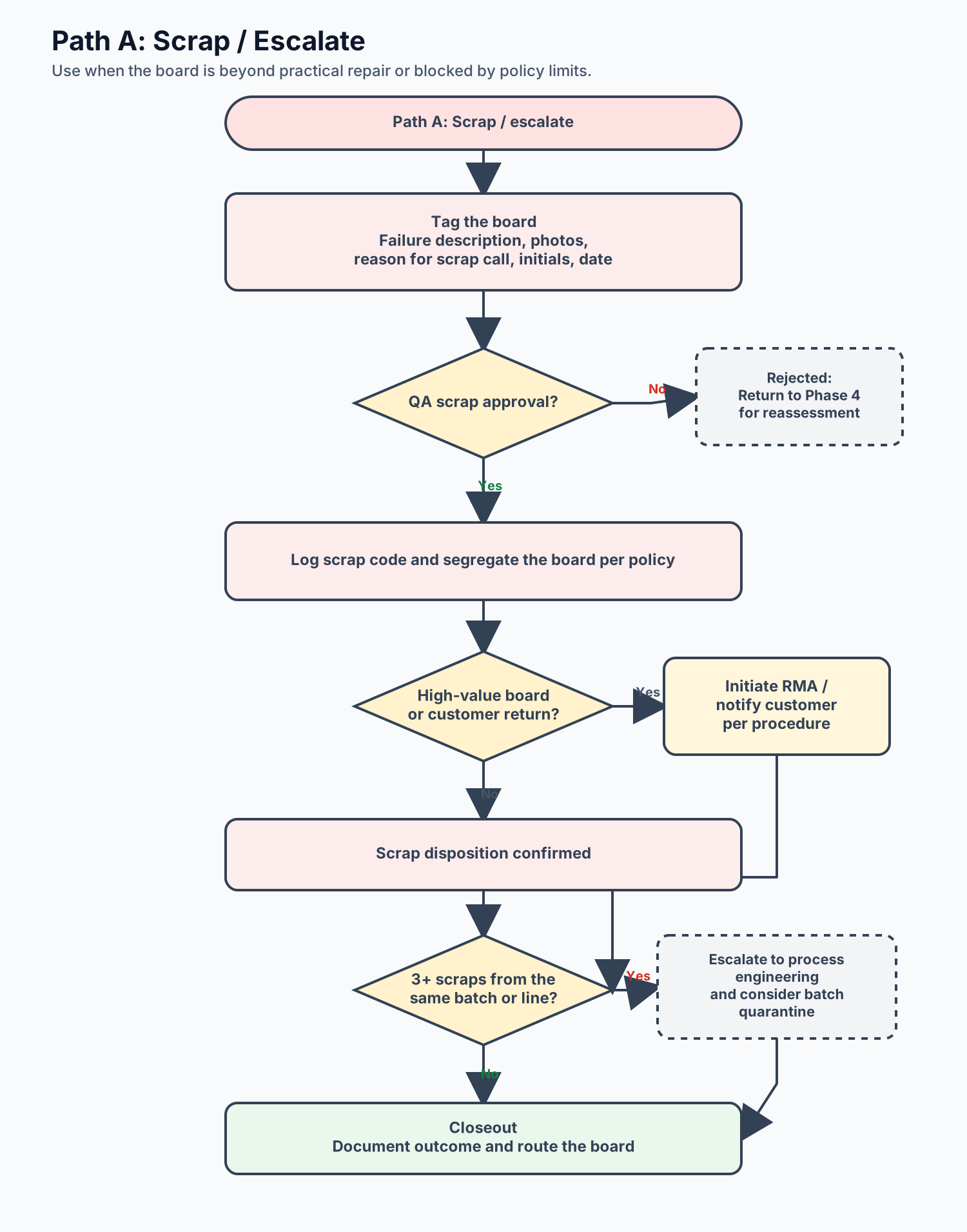
PATH B: REWORK
ESD-safe tool reminders in this rework path are tied to the ESD control sources cited for the complete flowchart.1
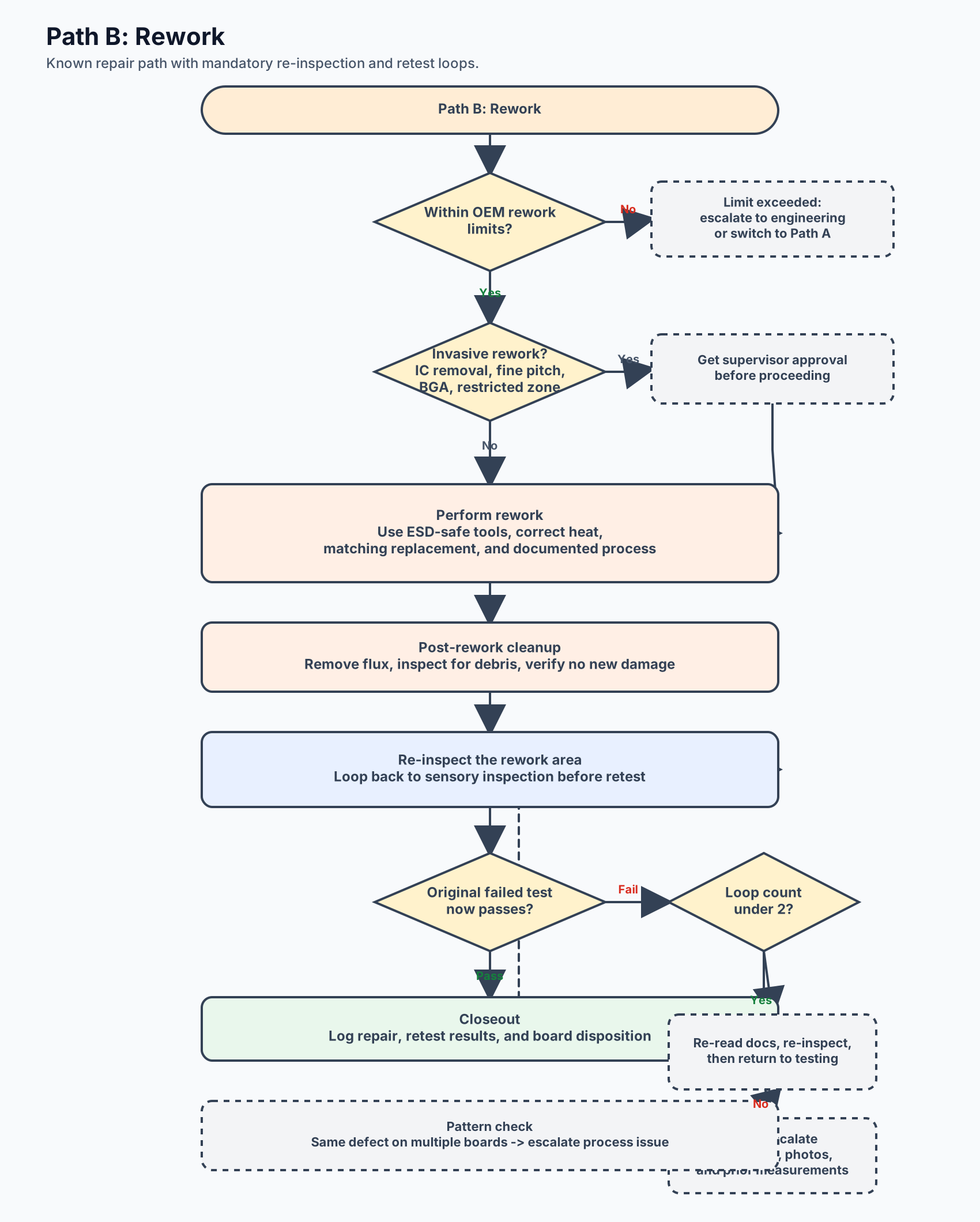
PATH C: RETEST
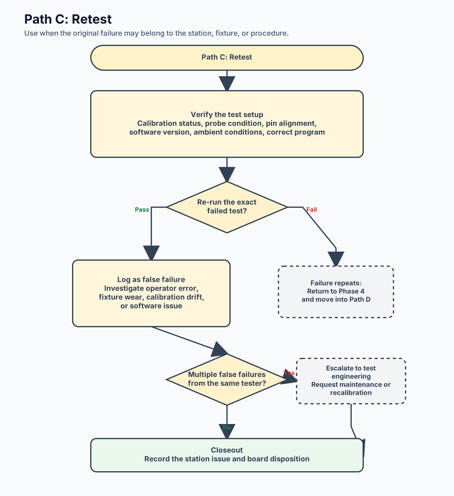
PATH D: DEBUG (Component-Level Diagnosis)
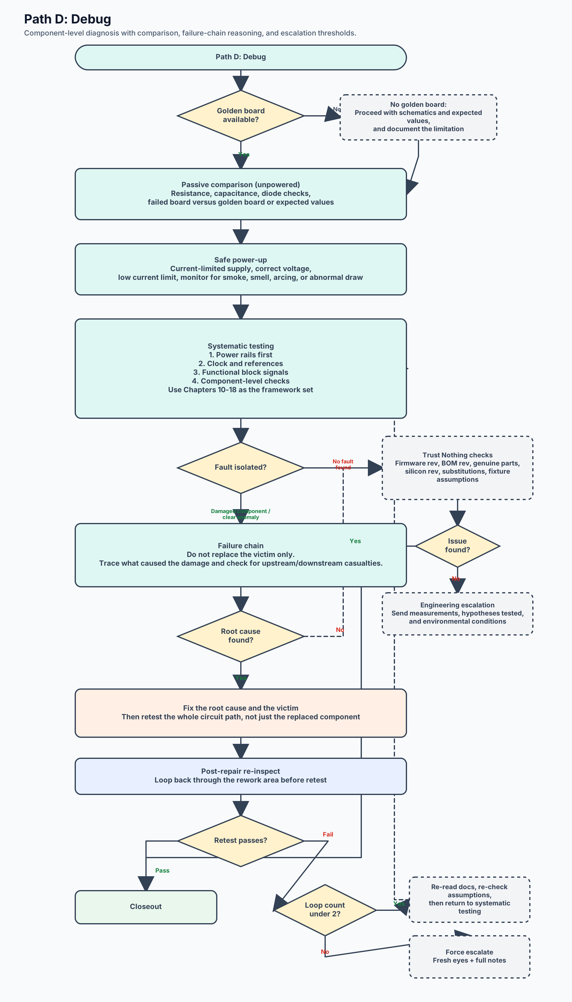
CLOSEOUT (Every Path Ends Here)
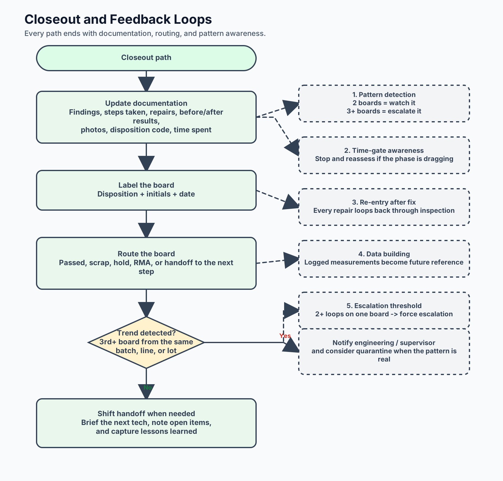
FEEDBACK LOOPS (Always Active)
These run in parallel with every phase — not sequential steps.
The feedback-loop cards are integrated into the closeout sheet above so the pullout keeps the always-active checks on the same page as disposition, documentation, routing, and escalation.
Cross-references: Ch 1 (flowchart introduction), Ch 2 (safety), Ch 3 (ESD), Ch 4 (documentation), Ch 5 (sensory inspection), Ch 6 (failure chain), Ch 7 (golden board), Ch 8 (trust nothing), Ch 10-14 (debug frameworks), Ch 15-20 (tools), Ch 29 (quality integration), Ch 30 (documentation and handoff)
Sources and notes
- EOS/ESD Association, "ANSI/ESD S20.20-2021," accessed 2026-04-22, https://www.esda.org/store/standards/product/314/ansiesd-s20-20-2021/; EOS/ESD Association, "EOS/ESD Fundamentals Part 1: An Introduction to ESD," accessed 2026-04-22, https://www.esda.org/esd-overview/esd-fundamentals/part-1-an-introduction-to-esd/.
Appendix B: Debug Checklists
Four checklists for the debug station. Print, laminate, and keep at your workstation. Use them every time — not because you'll forget, but because skipping steps is how boards come back.
Checklist 1: Receiving
Use when a board arrives at the debug station. Every board, every time. ESD handling items in these checklists follow the ESD control sources cited in Chapters 2 and 3.1
RECEIVING CHECKLIST
═══════════════════════════════════════════════════════════

□ ESD wrist strap connected and verified
□ ESD mat grounded
□ Board placed on ESD mat (not bare bench)

□ Board serial number / barcode scanned or recorded
□ Time and date logged
□ Your initials logged

□ Traveler present and matches board S/N
□ Test log present (which test failed, measured vs expected)
□ Failure description from test operator reviewed
□ Schematics available (correct revision)
□ BOM available (correct revision)
□ OEM special instructions reviewed (rework limits,
  restricted areas, required procedures)

□ Board revision marking matches documentation
□ Prior debug history checked (first trip or repeat?)
  If repeat: what was done previously? Same failure?

□ Missing documentation? ──> STOP. Escalate. Do not proceed.

Notes: ___________________________________________________
__________________________________________________________
__________________________________________________________
Cross-references: Ch 4 (Read Before You Touch), Ch 30 (Documentation and Handoff)
Checklist 2: Visual Inspection
Use during Phase 3 sensory inspection, before any power-up. Work systematically — corner to corner, both sides. Touch-check handling should stay inside the site's ESD control procedure.1
VISUAL INSPECTION CHECKLIST
═══════════════════════════════════════════════════════════

SOLDER DEFECTS
□ Solder bridges (especially fine-pitch QFP, SOIC, BGA)
□ Cold joints (dull, grainy, cracked solder)
□ Voids / insufficient solder (pad visible, thin fillet)
□ Tombstoned components (one end lifted)
□ Excess solder / solder balls
□ Head-in-pillow (BGA — may require X-ray)
□ Solder splash / debris between pins or pads

COMPONENT ISSUES
□ Missing components (empty pads vs BOM)
□ Wrong components (markings don't match BOM/refdes)
□ Reversed polarity — electrolytics, diodes, ICs
□ Misaligned components (rotated, shifted off pads)
□ Bent, folded, or bridged IC pins
□ Cracked or chipped components (especially MLCCs)
□ Damaged or missing connector housings

BOARD-LEVEL DAMAGE
□ Cracked substrate (visual/approved inspection; do not hand-flex)
□ Lifted pads or traces
□ Scratches or gouges through solder mask
□ Delamination (bubbling or separation of layers)
□ Burn marks or discoloration
□ Contamination (flux residue, foreign material, corrosion)

INCIDENTAL ODOR (DO NOT SNIFF OR LOCALIZE BY NOSE)
□ Unexpected acrid or ozone-like odor: isolate and follow site procedure

MECHANICAL CONDITION (DE-ENERGIZED, SUPPORTED, ESD-CONTROLLED)
□ Connector seating, latch, and housing condition
□ Visible component or joint movement only; do not rock packages
□ No hand-flexing, scraping, or touching damaged material

DOCUMENTATION
□ All findings photographed
□ All findings logged (traveler / MES / station log)
□ Board rev matches traveler and schematics

If inspection finds NOTHING: that's data. Log "visual clean"
and proceed to disposition.

Notes: ___________________________________________________
__________________________________________________________
__________________________________________________________
Cross-references: Ch 5 (Use Your Senses), Ch 22 (Solder Defects), Ch 23 (Component Failures)
Checklist 3: Power-Up
Use when entering powered debug (Path D). Never connect a suspect board to its normal power source without precautions. Keep the board in the protected work area during powered debug unless the site procedure says otherwise.1
POWER-UP CHECKLIST
═══════════════════════════════════════════════════════════

BEFORE APPLYING POWER
□ Visual inspection complete (Checklist 2)
□ No obvious shorts identified during inspection
□ Board is on ESD mat, strap connected
□ Bench supply set to correct voltage(s)
  Rail 1: ___V   Rail 2: ___V   Rail 3: ___V
□ Current limit and protection set from approved startup profile
  Rail 1: ___mA  Rail 2: ___mA  Rail 3: ___mA
□ Probe leads connected to measurement points
  BEFORE power is applied
□ Scope or meter ready to monitor during power-up

DURING POWER-UP
□ Apply power using the approved source and sequence
□ Watch voltage and current — compare to the authorized profile
  Expected: ___mA    Actual: ___mA
□ Unexpected limit, collapse, or spike? ──> STOP. Cause unknown.
  Investigate with unpowered methods before changing settings.
□ Smoke or smell? ──> POWER OFF IMMEDIATELY.
  Identify source. Do not re-power until resolved.
□ Arcing sound? ──> POWER OFF IMMEDIATELY.
□ Buzzing / whine? ──> Note it. May indicate
  oscillation or inductor saturation. Continue
  with caution.

POWERED MEASUREMENTS (in order)
□ 1. Power rails — all present? All within tolerance?
     Rail 1: expected ___V  measured ___V  □OK □FAIL
     Rail 2: expected ___V  measured ___V  □OK □FAIL
     Rail 3: expected ___V  measured ___V  □OK □FAIL
□ 2. Power rail ripple/noise (scope)
     Acceptable: < ___mV p-p
□ 3. Clock / oscillator signals present and clean
□ 4. Reference voltages in spec
□ 5. Proceed to signal-level debug (Ch 10-14)

IF MULTIPLE RAILS
□ Power rails sequentially to isolate which rail
  has the problem
□ Test each rail independently before combining

ALL MEASUREMENTS LOGGED? □ Yes

Notes: ___________________________________________________
__________________________________________________________
__________________________________________________________
Cross-references: Ch 17 (Current-Limited Power Supply), Ch 15 (Multimeter), Ch 16 (Oscilloscope), Ch 25 (Power and Ground Faults)
Checklist 4: Closeout
Use when disposition is complete — every path (pass, scrap, RMA, hold). If it's not documented, it didn't happen.
CLOSEOUT CHECKLIST
═══════════════════════════════════════════════════════════

DOCUMENTATION
□ All findings logged (traveler / MES / station log)
  - What was wrong
  - How it was found
  - What was measured (values, locations)
  - What was done (rework, retest, escalation)
□ All test results recorded (before and after)
□ All photos attached to record
□ Root cause identified and documented
  Root cause: _____________________________________________
□ If root cause NOT found: documented what was checked
  and ruled out
□ Disposition code entered
  □ Pass   □ Scrap   □ RMA   □ Hold   □ Escalated
□ Time spent recorded: _____ minutes

LABELING
□ Disposition label applied to board
  ("Debug Complete — Passed" / "Scrap" /
   "Hold for Engineering" / "RMA")
□ Your initials + date on label
□ If reworked: rework indicator applied per OEM
  requirements

ROUTING
□ Board routed to correct destination:
  □ Pass  ──> Pack-out / next production step
  □ Scrap ──> Scrap bin (QA-approved)
  □ Hold  ──> Hold area, engineering notified
  □ RMA   ──> RMA staging area

PATTERN CHECK
□ Does this board fit a trend?
  Same failure seen on other boards from same
  batch / line / lot / date code?
  □ No trend identified
  □ Possible trend ──> flagged in system,
    engineering / supervisor notified
  □ Confirmed trend ──> quarantine action initiated

SHIFT HANDOFF (if applicable)
□ Open items briefed to next tech
□ Boards in progress clearly marked with status
□ Debug notes legible and complete for continuation

SELF-REVIEW
□ Lessons learned noted for personal reference
□ Any new golden board data logged for future use
□ Any tool or supply issues flagged (probes worn,
  solder low, etc.)

Notes: ___________________________________________________
__________________________________________________________
__________________________________________________________
Cross-references: Ch 29 (Quality Integration), Ch 30 (Documentation and Handoff), Ch 31 (Communication and Escalation)
Sources and notes
- EOS/ESD Association, "ANSI/ESD S20.20-2021," accessed 2026-04-22, https://www.esda.org/store/standards/product/314/ansiesd-s20-20-2021/; EOS/ESD Association, "EOS/ESD Fundamentals Part 1: An Introduction to ESD," accessed 2026-04-22, https://www.esda.org/esd-overview/esd-fundamentals/part-1-an-introduction-to-esd/.
Appendix C: Toolkit Quick Reference
Mid-debug lookup table. You have a symptom — which tool do you grab and what do you do with it?
Tool Selection by Symptom
| Symptom | Recommended Tool | What to Measure | What the Result Means |
|---|---|---|---|
| Board completely dead — no power | DMM | DC voltage at input connector, then at each regulator output | No voltage at input = power path open or supply problem. Voltage at input but not output = regulator fault, blown fuse, or shorted rail |
| Board dead — power present but nothing runs | DMM, then Scope | DC rails at ICs, then clock signals | Rails present but clock missing = crystal/oscillator fault. Rails wrong = power section. Rails and clocks good = MCU or firmware |
| Current draw too high (short suspected) | Bench Supply (current-limited) | Current draw as you ramp voltage slowly | Current spikes at low voltage = hard short. Climbs linearly = resistive short. Normal at first, spikes at specific voltage = component breakdown |
| Current draw too low (open suspected) | DMM | Resistance along power path, continuity through traces and vias | Open reads >1M where it should read low ohms. Compare to golden board at same point |
| Voltage rail low but present | DMM + Scope | DC level, then AC ripple on the rail | DC low with clean rail = regulator output issue, loaded rail, or resistive connection. DC low with excessive ripple = regulator instability or bad output cap |
| Voltage rail noisy / oscillating | Scope | AC ripple at regulator output, then input | High-frequency oscillation = feedback instability (output cap ESR, compensation). Low-frequency ripple = input supply issue or load transient |
| Component runs hot | Thermal Camera | Surface temperature, compare to golden board | Hotter than golden = excess current through component (short downstream, component failing, wrong value). Cooler than golden = not conducting (open joint, dead part) |
| Component not heating up (should be) | Thermal Camera | Surface temperature under load | Cold component that should be warm = no current flow. Check connections, check that the component is receiving its drive/enable signal |
| Signal absent (dead output) | Scope | Signal at source, then move downstream | Signal present at source but dies somewhere = follow it until it drops. Signal absent at source = source circuit fault |
| Signal present but wrong shape | Scope | Waveform shape, amplitude, frequency, rise/fall times | Clipped = supply rail issue or saturation. Noisy = coupling from adjacent circuit or ground bounce. Slow edges = loading or capacitive issue |
| Signal present but wrong amplitude | Scope | Amplitude at each stage, compare to golden board | Drops at a specific stage = that stage's gain element is faulty. Gradual loss = loading issue or impedance mismatch |
| Digital comms failure (SPI, I2C, UART) | Scope, then Logic Analyzer | Signal presence and quality first (scope), then decode protocol (analyzer) | Scope shows activity but comms fail = protocol-level issue (wrong baud, wrong address, stuck line). No activity on scope = hardware fault (pull-ups, trace, driver IC) |
| I2C bus stuck low | DMM + Scope | Voltage on SDA/SCL lines (DMM), then activity (scope) | Both stuck low = bus contention or short to ground. One stuck = specific device holding line. Neither stuck = intermittent — use logic analyzer for long capture |
| Intermittent failure — thermal | Thermal Camera + Heat Gun + Freeze Spray | Monitor board thermally while applying localized heat or cold | Failure appears with heat = thermal-sensitive component or cracked joint that opens when hot. Failure appears with cold = component works marginally warm, fails cold |
| Intermittent failure — mechanical | DMM (continuity) | Continuity while flexing board or tapping components | Continuity breaks during flex = cracked trace or joint. Breaks during tap = loose component or connector |
| Suspect capacitor (bulging, cracked, or ESR drift) | LCR Meter | Capacitance and ESR at 1kHz or 100kHz (out of circuit) | Low capacitance = degraded or failed dielectric. High ESR = internal resistance increase (common electrolytic aging failure). Both in spec = cap is probably OK |
| Suspect semiconductor junction | DMM (diode mode) or Curve Tracer | Forward voltage drop in diode mode; V-I curve on curve tracer | Short reads ~0V both directions. Open reads OL both directions. Normal diode: 0.2-0.4V (Schottky), 0.5-0.7V (silicon). Curve tracer shows junction characteristics for comparison |
| Suspect passive (resistor or inductor value drift) | DMM or LCR Meter | Resistance (DMM, out of circuit preferred) or inductance (LCR meter) | Out of tolerance = replace and trace failure chain for root cause (why did it drift — overheating? overcurrent?). In-circuit readings may be misleading due to parallel paths |
| BGA or fine-pitch IC solder suspect | Boundary Scan (JTAG) | Pin-level connectivity through JTAG chain | Open pins show in boundary scan test. Shorts between adjacent pins show as stuck values. Requires JTAG access and test vectors |
| Need to verify IC pin connections without probing | Boundary Scan (JTAG) | JTAG chain integrity, then individual pin toggling | Chain break = open connection on JTAG pins. Pin test failure = solder fault on that specific pin. Non-JTAG pins can sometimes be tested via internal IC connections |
| Need to test downstream circuit with dead upstream | Function Generator (Signal Injection) | Inject known signal at safe point, monitor downstream response | Downstream works with injected signal = upstream fault. Downstream fails = fault is downstream of injection point |
Tool Capabilities Summary
| Tool | Measures | Strengths | Watch Out For |
|---|---|---|---|
| DMM | DC/AC voltage, resistance, continuity, diode forward voltage, capacitance (basic) | Fast, always available, first-reach tool | In-circuit resistance misleads (parallel paths). Phantom voltage on floating nodes. Autoranging delay misses transients. Loading effect on high-impedance circuits |
| Oscilloscope | Waveform shape, amplitude, frequency, timing, noise, ripple | Shows what the meter can't — AC behavior, transients, signal quality. Dual-channel comparison to golden board | Probe compensation matters. Ground lead inductance adds ringing on fast signals. Bandwidth limit vs signal frequency. AC vs DC coupling selection |
| Bench Supply (current-limited) | Controlled voltage with current monitoring | Protects the board from further damage. Current draw is diagnostic — tells you loading before you probe. Multiple rails can be powered independently | Don't exceed board's rated voltage. Set current limit before connecting. Watch for inrush on boards with large capacitor banks |
| Thermal Camera | Surface temperature distribution | Finds hot spots (overcurrent) and cold spots (no current) that electrical measurements miss. Fast, non-contact, whole-board view | Shows surface temperature, not junction temperature. Emissivity differences between materials affect accuracy. Reflective surfaces read wrong. Airflow affects readings |
| LCR Meter | Inductance, capacitance, resistance, ESR, impedance at specific frequencies | Accurate passive component measurement that DMM can't match. ESR measurement critical for capacitor health. Frequency-dependent measurements reveal defects | Must measure out of circuit for accuracy (parallel paths). Component must be discharged. Lead compensation needed for low values |
| Logic Analyzer | Digital signal timing, protocol decode (SPI, I2C, UART, CAN, etc.) | Long capture time — catches intermittent protocol errors. Decodes what the scope can only show as activity. Multiple channels simultaneously | Setup complexity. Threshold voltage must match logic family. Sample rate must be high enough for the protocol speed. Doesn't show analog signal quality |
| Curve Tracer | V-I characteristics of semiconductor junctions | Compares junctions directly — matched pairs, suspect vs known-good. Shows breakdown voltage, leakage, junction quality. No power-up needed | Requires out-of-circuit measurement for clean results. Limited to two-terminal characterization per test. Learning curve on interpreting traces |
| Function / Signal Generator | Produces test signals (sine, square, pulse, arbitrary) for injection | Tests downstream circuits without a working upstream. Controlled amplitude and frequency. Sweep capability finds resonant issues | Impedance mismatch can load or damage circuits. Don't exceed input ratings of the circuit under test. Output impedance affects delivered amplitude |
Quick Decision: Which Tool First?
Board arrives at debug ──> DMM first (voltage checks)
                      │
                      ├── Dead board? ──> Bench supply (current-limited power-up)
                      │
                      ├── Signal issue? ──> Scope (waveform check)
                      │
                      ├── Running hot? ──> Thermal camera
                      │
                      ├── Comms failure? ──> Scope first, then logic analyzer
                      │
                      ├── Suspect passive? ──> LCR meter (out of circuit)
                      │
                      ├── Suspect semiconductor? ──> DMM diode mode,
                      │                              then curve tracer
                      │
                      ├── BGA/fine-pitch? ──> Boundary scan if available
                      │
                      └── Dead upstream, need to test downstream?
                           ──> Function generator (signal injection)
Cross-references: Ch 15 (DMM), Ch 16 (Oscilloscope), Ch 17 (Bench Supply), Ch 18 (Thermal Imaging), Ch 20 (Other Essential Tools), Ch 10 (Half-Split), Ch 11 (Signal Tracing), Ch 12 (Signal Injection)
Appendix D: Common Component Markings and Packages
Quick reference for identifying what's on the board. When the BOM says one thing and the marking says another, this appendix helps you decode what you're actually looking at.
This appendix summarizes common marking conventions for training and bench triage. Marking systems vary by manufacturer, package, date code, and product family; the BOM, approved vendor list, reel label, and manufacturer datasheet control the final identification.1
SMD Resistor Codes
3-Digit Code (Most Common)
First two digits = significant figures. Third digit = multiplier (number of zeros).
| Marking | Value | Marking | Value |
|---|---|---|---|
| 100 | 10 ohm | 472 | 4.7K ohm |
| 101 | 100 ohm | 473 | 47K ohm |
| 102 | 1K ohm | 510 | 51 ohm |
| 103 | 10K ohm | 511 | 510 ohm |
| 104 | 100K ohm | 681 | 680 ohm |
| 105 | 1M ohm | 682 | 6.8K ohm |
| 150 | 15 ohm | 750 | 75 ohm |
| 151 | 150 ohm | 751 | 750 ohm |
| 220 | 22 ohm | 822 | 8.2K ohm |
| 221 | 220 ohm | 000 or 0 | 0 ohm (jumper) |
| 222 | 2.2K ohm | R10 | 0.10 ohm |
| 330 | 33 ohm | R47 | 0.47 ohm |
| 331 | 330 ohm | 1R0 | 1.0 ohm |
| 332 | 3.3K ohm | 4R7 | 4.7 ohm |
| 470 | 47 ohm | 10R | 10 ohm |
| 471 | 470 ohm |
"R" indicates decimal point. 4R7 = 4.7 ohm. R10 = 0.10 ohm.
4-Digit Code (1% Precision Resistors)
First three digits = significant figures. Fourth digit = multiplier.
| Marking | Value | Marking | Value |
|---|---|---|---|
| 1001 | 1.00K ohm | 4702 | 47.0K ohm |
| 1002 | 10.0K ohm | 4703 | 470K ohm |
| 1003 | 100K ohm | 1000 | 100 ohm |
| 1004 | 1.00M ohm | 1500 | 150 ohm |
| 2200 | 220 ohm | 2201 | 2.20K ohm |
| 2202 | 22.0K ohm | 3301 | 3.30K ohm |
| 3300 | 330 ohm | 6801 | 6.80K ohm |
| 4700 | 470 ohm | 1000 | 100 ohm |
EIA-96 Code (1% Resistors, Compact Marking)
Two-digit number + letter. The number maps to a value from the EIA-96 table. The letter is the multiplier.
Multiplier letters:
| Letter | Multiplier | Letter | Multiplier |
|---|---|---|---|
| Z | 0.001 | B | 10 |
| Y or R | 0.01 | C | 100 |
| X or S | 0.1 | D | 1,000 |
| A | 1 | E | 10,000 |
| F | 100,000 |
EIA-96 value codes (partial — most common):
| Code | Value | Code | Value | Code | Value | Code | Value |
|---|---|---|---|---|---|---|---|
| 01 | 100 | 13 | 133 | 25 | 178 | 37 | 237 |
| 02 | 102 | 14 | 137 | 26 | 182 | 38 | 243 |
| 03 | 105 | 15 | 140 | 27 | 187 | 39 | 249 |
| 04 | 107 | 16 | 143 | 28 | 191 | 40 | 255 |
| 05 | 110 | 17 | 147 | 29 | 196 | 41 | 261 |
| 06 | 113 | 18 | 150 | 30 | 200 | 42 | 267 |
| 07 | 115 | 19 | 154 | 31 | 205 | 43 | 274 |
| 08 | 118 | 20 | 158 | 32 | 210 | 44 | 280 |
| 09 | 121 | 21 | 162 | 33 | 215 | 45 | 287 |
| 10 | 124 | 22 | 165 | 34 | 221 | 46 | 294 |
| 11 | 127 | 23 | 169 | 35 | 226 | 47 | 301 |
| 12 | 130 | 24 | 174 | 36 | 232 | 48 | 309 |
| Code | Value | Code | Value | Code | Value | Code | Value |
|---|---|---|---|---|---|---|---|
| 49 | 316 | 61 | 422 | 73 | 562 | 85 | 750 |
| 50 | 324 | 62 | 432 | 74 | 576 | 86 | 768 |
| 51 | 332 | 63 | 442 | 75 | 590 | 87 | 787 |
| 52 | 340 | 64 | 453 | 76 | 604 | 88 | 806 |
| 53 | 348 | 65 | 464 | 77 | 619 | 89 | 825 |
| 54 | 357 | 66 | 475 | 78 | 634 | 90 | 845 |
| 55 | 365 | 67 | 487 | 79 | 649 | 91 | 866 |
| 56 | 374 | 68 | 499 | 80 | 665 | 92 | 887 |
| 57 | 383 | 69 | 511 | 81 | 681 | 93 | 909 |
| 58 | 392 | 70 | 523 | 82 | 698 | 94 | 931 |
| 59 | 402 | 71 | 536 | 83 | 715 | 95 | 953 |
| 60 | 412 | 72 | 549 | 84 | 732 | 96 | 976 |
Example: Marking "68C" = code 68 (499) x 100 = 49.9K ohm.
SMD Capacitor Markings
Capacitors are harder to identify than resistors. Many SMD ceramic caps have no marking at all — especially 0402 and 0603 sizes. When markings are present:
Ceramic Capacitors (When Marked)
Some larger ceramic caps use a 3-digit code similar to resistors, but the value is in picofarads (pF).
| Marking | Value | Marking | Value |
|---|---|---|---|
| 100 | 10 pF | 473 | 47 nF (0.047 uF) |
| 101 | 100 pF | 474 | 470 nF (0.47 uF) |
| 102 | 1 nF (1,000 pF) | 104 | 100 nF (0.1 uF) |
| 103 | 10 nF (0.01 uF) | 105 | 1 uF |
| 104 | 100 nF (0.1 uF) | 220 | 22 pF |
| 222 | 2.2 nF | 330 | 33 pF |
| 223 | 22 nF | 470 | 47 pF |
| 224 | 220 nF (0.22 uF) | 471 | 470 pF |
| 472 | 4.7 nF |
Key difference from resistors: Capacitor codes give values in picofarads. Resistor codes give values in ohms.
Electrolytic / Tantalum SMD Capacitors
Typically marked with capacitance value and voltage rating directly:
- "47" and "16V" = 47 uF, 16V rated
- "100 6V" = 100 uF, 6V rated
- Single letter voltage codes may appear:
| Letter | Voltage | Letter | Voltage |
|---|---|---|---|
| e | 2.5V | G | 4V |
| J | 6.3V | A | 10V |
| C | 16V | D | 20V |
| E | 25V | V | 35V |
| H | 50V |
If There's No Marking
This is common. If you need to verify a capacitor value, measure it:
- Out of circuit with an LCR meter for accurate readings
- In circuit with a DMM capacitance mode gives rough confirmation only (parallel paths affect reading)
- Compare to the BOM for expected value
- Compare to the golden board at the same location
IC Package Types and Pin Numbering
SOT-23 (3-pin and 5-pin)
SOT-23-3                    SOT-23-5
(transistors, voltage       (voltage regulators,
 references, diodes)         op-amps, small ICs)

  ┌────────┐                  ┌────────┐
  │ •      │                  │ •      │
1 ┤        ├ 3              1 ┤        ├ 5
  │        │                2 ┤        ├ 4
2 ┤        │                  │        ├ 3
  └────────┘                  └────────┘

Pin 1: dot, stripe, or      Pin 1: dot, stripe, or
chamfered corner             chamfered corner
SOIC (8-pin shown — scales to 14, 16, etc.)
SOIC-8
        ┌──── notch / dot
        ▼
  ┌─────•─────┐
1 ┤           ├ 8
2 ┤           ├ 7
3 ┤           ├ 6
4 ┤           ├ 5
  └───────────┘

Pin 1: identified by dot, notch, or chamfer at one end.
Count counterclockwise from pin 1 (viewed from top).
QFP / TQFP / LQFP (quad flat pack)
LQFP-48 (example)
                  Pin 1 indicator
                     (dot/chamfer)
             ┌──────•──────┐
             │ 37  ...  48 │
        36 ──┤             ├── 25
        ...  │             │  ...
        25 ──┤             ├── 13
             │  1  ...  12 │
             └─────────────┘

Pin 1: corner dot, chamfer, or notch.
Count counterclockwise from pin 1 (viewed from top).
Pin count varies: 32, 44, 48, 64, 80, 100, 128, 144, 176, 208.
Pitch: 0.4mm, 0.5mm, 0.65mm, 0.8mm (check datasheet).
QFN / DFN (quad flat no-lead)
QFN-32 (example)
          ┌────────────────┐
          │  •             │  ← Pin 1 dot
          │                │
          │   Exposed pad  │  ← Thermal/ground pad
          │   (center)     │     on underside
          │                │
          └────────────────┘

Pads are on the underside edges — no visible leads.
Pin 1: dot on top surface, chamfer on corner, or
       one pad slightly offset.
Exposed center pad is usually ground or thermal.
INSPECT WITH MAGNIFICATION — pads are hidden.
BGA-like solder issues possible on center pad.
BGA (Ball Grid Array)
BGA (bottom view — ball side up)

    A  B  C  D  E  F  ...
  ┌─────────────────────┐
1 │ ●  ●  ●  ●  ●  ●   │
2 │ ●  ●  ●  ●  ●  ●   │
3 │ ●  ●  ●  ●  ●  ●   │
4 │ ●  ●  ●  ●  ●  ●   │
  └─────────────────────┘

Pin A1: identified by dot on package top or
        asymmetric corner marking.
Columns: letters (A, B, C, ...).
Rows: numbers (1, 2, 3, ...).
Example: "Ball C3" = column C, row 3.
Pitch: 0.4mm, 0.5mm, 0.65mm, 0.8mm, 1.0mm, 1.27mm.

CANNOT BE VISUALLY INSPECTED for solder joints.
Requires X-ray or boundary scan (JTAG) for verification.
Polarity Indicators
Getting polarity wrong kills components and wastes debug time. Know the marks.
Electrolytic Capacitors (Through-Hole)
  ──┤├──        Longer lead = POSITIVE (on new parts)
                Stripe with minus signs (–) = NEGATIVE side
Electrolytic / Tantalum Capacitors (SMD)
Aluminum Electrolytic SMD:
  ┌────────┐
  │ ▓▓▓  ○ │     Stripe/bar marks NEGATIVE (cathode)
  └────────┘     (Opposite of through-hole convention!)
  (-)    (+)

Tantalum SMD:
  ┌────────┐
  │ ▓▓     │     Stripe/bar marks POSITIVE (anode)
  └────────┘     (Opposite of aluminum electrolytic!)
  (+)    (-)

CRITICAL: Tantalum and aluminum electrolytics use OPPOSITE
          marking conventions. Tantalum stripe = positive.
          Aluminum stripe = negative. Verify with datasheet.
Diodes
Through-hole:         SMD:
  ──|◄──               ┌──────┐
  A    K               │ ▓▓   │
                       └──────┘
Band/stripe marks      K      A
CATHODE (negative)
                       Band marks CATHODE

Cathode = the bar side of the schematic symbol.
Current flows from Anode to Cathode.
ICs
Pin 1 indicators (any combination may be present):

  Dot near pin 1    ── Most common
  Notch at one end  ── Pin 1 is left of notch (top view)
  Chamfered corner  ── Corner near pin 1 is beveled
  Stripe or bar     ── Near pin 1 end

When in doubt: check the datasheet and compare
to the PCB silkscreen / assembly drawing.
LEDs
Through-hole:
  Longer lead = ANODE (+)
  Flat side of lens = CATHODE (-)

SMD:
  Green dot or T-mark = CATHODE on many packages
  Check datasheet — conventions vary by manufacturer
Common Manufacturer Logos
Recognizing these on ICs helps identify the manufacturer and look up datasheets.
| Logo Description | Manufacturer | Common Products |
|---|---|---|
| Stylized "ti" in oval frame | Texas Instruments (TI) | Voltage regulators, op-amps, ADCs/DACs, MSP430/C2000 MCUs, logic ICs |
| Interlocked "NXP" | NXP Semiconductors | ARM MCUs (LPC, i.MX), NFC/RFID, automotive ICs, MOSFET drivers |
| Upward arrow / "ST" in rectangle | STMicroelectronics | STM32 MCUs, power MOSFETs, regulators, motor drivers, MEMS sensors |
| Stylized "M" with arrow | Microchip Technology | PIC/AVR/SAM MCUs, serial EEPROMs, Ethernet controllers, analog ICs |
| Infinity symbol / "ADI" | Analog Devices (ADI) | Precision ADCs/DACs, op-amps, IMUs, signal conditioning, power management |
| Interlocked "IFX" or old Siemens "S" | Infineon | Power MOSFETs (OptiMOS), gate drivers, automotive MCUs (AURIX), sensors |
| Circle with arrow through it | ON Semiconductor (onsemi) | MOSFETs, diodes, voltage regulators, LED drivers, image sensors |
| Stylized "M" (block letter) | Murata | MLCCs, inductors, EMI filters, ceramic resonators |
| "TDK" | TDK | Inductors, ferrites, MLCCs, EMI filters |
| "Y" with three branches | Yageo | Resistors, MLCCs, inductors (very common in CM environments) |
| "W+" or Vishay text | Vishay | Resistors, capacitors, diodes, MOSFETs, optocouplers |
| "MX" or Macronix text | Macronix | Serial NOR flash memory |
| "W" in circle | Winbond | Serial flash memory, DRAM, specialty memory |
| Samsung text or "SEC" | Samsung | DRAM, NAND flash, eMMC, PMIC |
| "SK" + Hynix text | SK Hynix | DRAM, NAND flash |
| "MT" or Micron text | Micron | DRAM, NAND flash, NOR flash |
When a marking is unreadable or unfamiliar:
- Compare to the BOM — the part number tells you the manufacturer
- Cross-reference the package and pin count
- Check manufacturer's marking guide (most publish one as an app note)
- If markings don't match the BOM at all, consider counterfeit — escalate per Ch 81
Cross-references: Ch 5 (Use Your Senses — visual inspection), Ch 8 (Trust Nothing — counterfeits), Ch 23 (Component Failures), Ch 26 (Design and Assembly Mismatches)
Sources and notes
- DigiKey Electronics, "SMD Resistor Code Calculator," accessed 2026-04-23, https://www.digikey.com/en/resources/conversion-calculators/conversion-calculator-smd-resistor-code; KEMET, "Tantalum Surface Mount Capacitors - Standard Tantalum," accessed 2026-04-23, https://content.kemet.com/datasheets/KEM_T2024_T489.pdf.
Appendix E: Failure Mode Quick Reference
One section per component type. Each section is designed to fit on a single page for fast lookup during debug. When you suspect a specific component, find its section and work through the table.
This appendix is a general troubleshooting quick reference, not a substitute for device-specific ratings, acceptance standards, or failure-analysis evidence. Use the tables to choose what to inspect next, then verify exact limits against the schematic, BOM, datasheet, workmanship standard, and golden board.2
Resistors
| Failure Mode | Symptoms on the Board | Likely Root Cause | How to Measure |
|---|---|---|---|
| Open (most common) | Circuit function lost. Voltage present on one side, absent on the other. Infinite resistance across part. | Cracked body (mechanical stress, reflow thermal shock). Cracked solder joints. Trace lift at pad. | DMM resistance: should read nominal value. OL = open. Compare to golden board. Visual: look for hairline cracks, especially on 0402/0603. |
| Drift (value shifted) | Circuit works but out of spec. Marginal test failures. Voltage or current slightly off expected. | Overheating from sustained overcurrent. Aging under stress. Wrong value placed (assembly error). | DMM resistance out of circuit: compare to marked value. In-circuit reading may be misleading (parallel paths). If drifted, trace the failure chain — why was it overstressed? |
| Short (rare) | Unexpected connection between pads. Usually manifests as a downstream overcurrent. | Almost never the resistor itself. Check for solder bridge across pads, conductive contamination (flux, debris), or PCB damage between traces. | DMM resistance: reads near 0 ohm. Visual inspection under magnification. Clean board and remeasure if contamination suspected. |
Key point: A burnt or open resistor is usually the victim, not the cause. Trace the failure chain (Ch 6).2
Capacitors — Electrolytic (Aluminum)
| Failure Mode | Symptoms on the Board | Likely Root Cause | How to Measure |
|---|---|---|---|
| ESR increase (most common aging failure) | Power rail ripple increases. Regulator oscillates. Voltage droop under load. Board runs hotter than expected. | Age and thermal cycling. Operating at or above rated temperature. Electrolyte drying out over time. | LCR meter at 100kHz: ESR above datasheet maximum. Scope on power rail: increased ripple at switching frequency. Compare to golden board. |
| Capacitance loss | Filtering degraded. Timing circuits drift. Decoupling ineffective. | Same as ESR increase — electrolyte degradation. Often accompanies ESR rise. | LCR meter: capacitance below rated value. If >20% low, replace. |
| Short (dielectric breakdown) | Power rail shorted to ground. Fuse blown. Regulator in current limit or thermal shutdown. Board draws excessive current at power-up. | Overvoltage (exceeded rating). Reverse polarity installation. Voltage derating exceeded. Defective lot. | DMM resistance across cap: near 0 ohm = shorted. On current-limited supply: current spikes when powering the rail this cap is on. Remove cap and remeasure rail. |
| Open (lead failure) | Loss of filtering on that node. AC noise increases. Same symptoms as missing cap. | Vibration cracking lead wire. Poor solder joint on SMD aluminum electrolytic. | LCR meter: reads very low or zero capacitance. DMM: no continuity through cap. |
| Venting / bulging | Visible bulge on top, electrolyte residue on board, possible burnt smell. | Overvoltage, reverse polarity, or excessive ripple current causing internal heating. | Visual first. If top vent is pushed out or ruptured, replace. Check for cause — verify rail voltage is within cap's rating. Check polarity. |
Key point: Electrolytic caps are a leading cause of failures in aged or thermally stressed assemblies. Check ESR, not just capacitance.
Capacitors — MLCC (Multilayer Ceramic)
| Failure Mode | Symptoms on the Board | Likely Root Cause | How to Measure |
|---|---|---|---|
| Cracked (mechanical — most common) | Intermittent behavior. Works on bench, fails under vibration or thermal cycling. May short intermittently. | Board flex during depaneling, fixture clamping, or connector insertion. Thermal shock from rework. Large body size (0805+) more susceptible. | Visual under magnification: look for hairline cracks, especially at solder fillets. May need to remove to see crack on underside. If suspected, replace and retest. |
| Short (crack-induced) | Rail shorted to ground (if bypass cap). Excessive current draw. Regulator output collapses. | Crack propagates through internal electrode layers, creating a conductive path. Flex crack + moisture ingress. | DMM resistance across cap: near 0 ohm. Remove cap, remeasure rail — if rail recovers, cap was the short. Inspect removed cap under magnification. |
| DC bias derating (design-related) | Decoupling less effective than expected. Higher ripple. Not a "failure" — it's physics. | High-K ceramic dielectric (X5R, X7R) loses capacitance as DC bias increases. A 10uF 0805 cap at rated voltage may provide only 3-4uF actual. | LCR meter at 0V bias will read full value. Effective capacitance under DC bias is lower. This is a design issue — escalate to engineering if suspected. |
| Open | Missing decoupling on that node. Increased noise on nearby IC. May cause IC malfunction. | Tombstone during reflow (one end open). Solder void underneath. Cracked and separated internally. | DMM capacitance: reads 0 or very low. LCR meter confirms. Visual: check for tombstone or poor joint. |
Key point: MLCC cracks are mechanical failures — look at board handling, fixture design, and depaneling process if you see a pattern.
Inductors
| Failure Mode | Symptoms on the Board | Likely Root Cause | How to Measure |
|---|---|---|---|
| Saturation (under load) | Switching regulator output drops or oscillates under load. Current ripple increases. Inductor runs hot. Efficiency drops. | Inductor undersized for actual current (design). Core material saturates at operating temperature. Higher ambient than rated. | Scope on switching node: current waveform goes triangular-to-sawtooth (asymmetric). Thermal camera: inductor hotter than expected. LCR meter shows reduced inductance at DC bias. |
| Winding short (turn-to-turn) | Reduced inductance. Regulator instability. Increased current draw. Inductor hot. | Manufacturing defect. Overcurrent event damaged insulation. Thermal degradation over time. | LCR meter: inductance below spec. DCR (DC resistance) lower than datasheet (shorted turns reduce both). Compare to golden board. |
| Open winding | Circuit dead — no current path through inductor. For power inductors: output rail absent. | Overcurrent event (fuse-like failure). Cracked solder joints. Wire bond failure in molded types. | DMM continuity: OL through inductor = open. Should read low ohms (DCR value from datasheet). |
| DCR increase | Voltage drop across inductor higher than expected. Efficiency drops. Inductor warm. | Degraded winding connections. Corrosion. Partial open. | DMM resistance: compare to datasheet DCR value. Should be milliohms to low ohms depending on type. Higher than spec = degraded. |
Key point: Inductor problems are often load-dependent. Test under actual operating conditions, not just on the bench with no load.
Diodes (Including Schottky, Zener, TVS)
ESD and overstress entries in this table are general diagnostic patterns; verify device-specific ratings and limits in the relevant datasheet.1
| Failure Mode | Symptoms on the Board | Likely Root Cause | How to Measure |
|---|---|---|---|
| Short (most common failure) | Protection diode: rail shorted to ground or clamped to wrong voltage. Rectifier: no rectification, DC appears on AC side. | Overvoltage / overcurrent event. ESD strike. Avalanche breakdown exceeded. Surge beyond TVS rating. | DMM diode mode: reads ~0V both directions = shorted. Curve tracer: flat line through origin. If protection diode shorted, check what it was protecting — the cause may still be present. |
| Open | Protection lost — vulnerable to next surge. Rectifier: no current flow, output dead. | Overcurrent (fuse-like failure). Bond wire failure. Severe thermal damage. | DMM diode mode: reads OL both directions = open. Curve tracer: no conduction in either direction. |
| Forward voltage drift | Slightly more or less voltage drop than expected. Marginal regulator output. | Thermal degradation. Junction damage from overheating. | DMM diode mode: compare Vf to datasheet nominal. Silicon: expect 0.5-0.7V. Schottky: 0.2-0.4V. Significant deviation = suspect. Compare to golden board. |
| Reverse leakage increase | Bias voltage bleeds through where it shouldn't. Leakage current heats the diode. Battery drain in sleep mode. | Thermal damage. ESD damage to junction. Aging under reverse bias stress. | Curve tracer: visible reverse leakage (current flow in reverse direction before breakdown). DMM may not detect small leakage — curve tracer is the right tool here. |
Key point: A shorted protection diode did its job. It saved something else. Find out what caused the event before replacing the diode and calling it fixed.
MOSFETs
MOSFET ESD and overstress entries should be checked against the specific part datasheet and the ESD handling references cited in Chapter 3.1
| Failure Mode | Symptoms on the Board | Likely Root Cause | How to Measure |
|---|---|---|---|
| Gate oxide failure (ESD — most common) | MOSFET stuck on (short drain-source) or stuck off (open). Gate no longer controls conduction. | ESD event on gate pin (gate oxide is thin, fragile). Can be latent — passes test initially, fails later. | DMM diode mode: check gate-source, gate-drain, drain-source. Shorted gate-source or gate-drain = oxide failure. Compare to known-good MOSFET readings. |
| Drain-source short | Load always powered (high-side) or ground rail pulled down (low-side). Excessive current through MOSFET. Board may smoke on power-up. | Overcurrent beyond SOA (safe operating area). Thermal runaway. Avalanche breakdown from inductive load spikes. Shoot-through in half-bridge configuration. | DMM diode mode: drain-source reads ~0V both ways = shorted (should show body diode ~0.5-0.7V in one direction, OL in other). |
| Rdson increase | MOSFET heats up more than expected. Voltage drop across MOSFET rises. Efficiency loss. | Thermal degradation from sustained overcurrent. Bond wire degradation. Die-level damage. | Compare drain-source voltage drop at known current to datasheet Rdson. Thermal camera: compare to golden board — hotter MOSFET at same load = degraded. |
| Gate drive failure (not the MOSFET itself) | MOSFET doesn't turn on or turns on sluggishly. Switching waveform wrong. | Gate driver IC failed. Gate resistor open or wrong value. Gate drive voltage too low (especially for logic-level MOSFETs). | Scope on gate pin: verify drive signal present, correct amplitude (check Vgs(th) in datasheet), correct timing. If gate signal is good but MOSFET doesn't respond, MOSFET is dead. |
Key point: MOSFETs are often victims of upstream failures (bad gate drive, inductive spikes, shoot-through from timing errors). Trace the failure chain before swapping.
ICs (General — MCUs, Regulators, Op-Amps, Logic, etc.)
IC failure signatures are generalized diagnostic patterns; cite the actual device datasheet when using a real part number or rating.1
| Failure Mode | Symptoms on the Board | Likely Root Cause | How to Measure |
|---|---|---|---|
| ESD damage | Intermittent or permanent failure on specific pins. Pin-specific malfunction while rest of IC works. Latch-up (IC draws excessive current, gets hot). | ESD event on I/O pin. Handling without ESD precautions. Unprotected connector pin exposed to ESD source. | DMM diode mode: check I/O pin to Vcc and GND. Compare to golden board. Abnormal readings on one pin suggest ESD damage. Boundary scan (JTAG) can detect pin-level failures on supported ICs. |
| Thermal failure | IC stops functioning above a temperature threshold. Erratic behavior under load. | Inadequate heatsinking. Thermal pad not soldered (especially QFN). Operating beyond thermal limits. Adjacent component heating. | Thermal camera: compare to golden board. If IC is hottest point on board, check power dissipation vs datasheet limits. Check thermal pad solder (X-ray for QFN/BGA). |
| Latch-up | IC suddenly draws high current, gets very hot. May damage IC permanently. | Input voltage exceeds supply rails (even briefly). ESD event. Power supply sequencing violation. | Current draw from IC power pins increases dramatically. Power off immediately — latch-up can be destructive. After power cycle, IC may or may not recover. If repeatable, investigate what triggers the overvoltage on the inputs. |
| Pin-specific failure | One function of a multi-function IC doesn't work. Others are fine. | Solder or interconnect fault, configuration, external loading, electrical overstress, ESD, or an internal device fault. | Test the function and pin under defined conditions. Verify connectivity, loading, protection parts, configuration, and expected response. A nonresponse can implicate the IC but does not identify an internal mechanism without further analysis. |
| Supply pin fault | IC completely dead. No response on any pin. | Solder fault on Vcc or GND pin. Decoupling cap failure starving the IC. Supply rail never reaching the IC. | DMM: verify voltage at IC supply pins (not just at the regulator output — check at the IC itself). Scope: check for noise/dropout on IC supply. |
| Wrong firmware / configuration | Hardware measures good. IC doesn't behave correctly. Outputs wrong or absent. | Programming error. Wrong firmware revision. Fuse bits misconfigured. Config registers not initialized. | Verify firmware version against build docs. Read device ID if accessible. Compare programming logs to BOM requirements. See Ch 8. |
Key point: Before replacing an IC, verify power, ground, clock, reset, and decoupling. Many "dead IC" diagnoses are actually support circuit failures.
Connectors
| Failure Mode | Symptoms on the Board | Likely Root Cause | How to Measure |
|---|---|---|---|
| Intermittent contact | Signal or power drops out sporadically. Passes one setup, fails in another. | Worn contacts, contamination, loss of normal force, fretting, damaged plating, or board-mount joint defects. | Inspect and measure under the connector's approved mating and mechanical-stimulus procedure. Compare contact resistance with the connector specification and a controlled reference; there is no universal one-ohm limit. |
| Cracked solder joints | Intermittent connection or visible movement at a board-mount termination. Multiple pins may be affected. | Mechanical stress from cable insertion/removal, thermal cycling, or an inadequate assembly process. | Inspect under magnification and use the approved mechanical-stimulus or fixture procedure while monitoring continuity. Do not push a powered connector by hand to declare a joint defective. |
| Bent or misaligned pins | Open on specific pins. Short between adjacent pins. Connector won't mate properly. | Handling damage. Misaligned during pick-and-place. Fixture damage. Mating force with misaligned cable. | Visual: compare pin alignment to known-good. DMM: check continuity on suspected pins. Check for shorts between adjacent pins. |
| Housing damage | Connector won't mate or retention fails. Intermittent due to loose fit. | Mechanical impact. Excessive insertion force. Wrong mating connector used. | Visual inspection. Compare to known-good connector. If housing is cracked or deformed, replace — mechanical damage affects electrical reliability. |
Key point: Connector failures are mechanical problems. Check seating, contacts, and solder joints before blaming the circuit.
Crystals and Oscillators
| Failure Mode | Symptoms on the Board | Likely Root Cause | How to Measure |
|---|---|---|---|
| No startup | MCU or comms IC won't boot. Clock signal absent. | Wrong load capacitor values (too high kills oscillation). Crystal damaged during reflow. Moisture absorption before assembly. PCB layout puts stray capacitance on crystal traces. | Scope on crystal pins: should see sinusoidal oscillation at rated frequency. No signal = not starting. Check load caps match datasheet recommendation. Compare to golden board. |
| Frequency drift | Timing-sensitive functions fail (UART baud rate errors, protocol timeouts, RTC drift). | Temperature outside rated range. Aging. Wrong load caps pulling frequency off-target. Board contamination on crystal traces adding parasitic capacitance. | Frequency counter or scope with frequency measurement. Compare to rated frequency. If drift exceeds spec (typically +/- 20-50 ppm), investigate load caps and board contamination. |
| Frequency pulling | Oscillation present but off-frequency. Comms work intermittently. | Load capacitance mismatch. One load cap missing, wrong value, or shorted. Crystal operating outside its specified load. | Scope: measure frequency precisely. Check both load caps (value and condition). Replace caps with correct values per crystal datasheet. Recheck frequency. |
| Spurious oscillation | Multiple frequencies present. Clock jitter. Erratic MCU behavior. | Layout issue (long traces to crystal, poor grounding). Contamination between crystal pins. Crystal damaged. | Scope: look for multiple frequency components or unstable waveform envelope. Clean board around crystal. Verify layout matches crystal manufacturer's recommendations. |
Key point: Crystal problems are often load cap problems. Verify both caps before replacing the crystal.
Cross-references: Ch 6 (The Failure Chain), Ch 15 (DMM), Ch 16 (Oscilloscope), Ch 18 (Thermal Imaging), Ch 20 (Other Essential Tools — LCR meter, curve tracer), Ch 22 (Solder Defects), Ch 23 (Component Failures), Ch 24 (Intermittent Failures), Ch 25 (Power and Ground Faults)
Sources and notes
- EOS/ESD Association, "EOS/ESD Fundamentals Part 1: An Introduction to ESD," accessed 2026-04-22, https://www.esda.org/esd-overview/esd-fundamentals/part-1-an-introduction-to-esd/. Use manufacturer datasheets for part-specific absolute maximum ratings, ESD ratings, curves, and package behavior.
- Editorial scope note for this manuscript. For ESD-related failure mechanisms, see EOS/ESD Association, "EOS/ESD Fundamentals Part 1: An Introduction to ESD," accessed 2026-04-23, https://www.esda.org/esd-overview/esd-fundamentals/part-1-an-introduction-to-esd/. For part-specific limits, use the relevant manufacturer datasheet.
Appendix F: Glossary
Production floor terminology. If you hear a word on the floor that you don't recognize, check here first. Standards-related terms should be cross-checked against the relevant standards body or manufacturer documentation before final publication.1
| Term | Definition |
|---|---|
| AOI | Automated Optical Inspection. Camera-based system that photographs every board after reflow and compares to a reference image. Catches missing parts, tombstones, bridges, misalignment. Does not catch internal defects (bad silicon, wrong firmware). |
| ATE | Automated Test Equipment. Any machine that tests boards automatically — includes ICT, flying probe, functional testers. The machines that generate your debug workload. |
| AWG | American Wire Gauge. Wire size standard. Lower number = thicker wire. Common in cable harnesses and test fixtures. |
| BGA | Ball Grid Array. IC package where solder balls on the underside connect to the PCB. Solder joints are invisible from the top — requires X-ray or boundary scan to verify. High pin count in small area. |
| BOM | Bill of Materials. The list of every component on the board — part number, value, reference designator, manufacturer, approved alternates. The BOM is your truth document. If the board doesn't match the BOM, something is wrong. |
| Boundary Scan | Test method using JTAG interface to verify IC pin connections without physical probing. Valuable for BGA and fine-pitch parts where you can't see or reach the joints. |
| CM | Contract Manufacturer. The company that builds boards for OEM customers. The production floor where you work. Builds to customer specs, not their own designs. |
| CTE | Coefficient of Thermal Expansion. How much a material expands when heated. Mismatched CTE between component and PCB causes solder joint stress during thermal cycling. Relevant to MLCC cracking and BGA reliability. |
| DCR | DC Resistance. The resistance of an inductor's winding measured at DC. Higher DCR = more power loss. Check against datasheet value — increase indicates degraded winding. |
| DFM | Design for Manufacturability. Engineering practice of designing boards that are easy to build correctly. Poor DFM creates recurring production defects. Not the tech's problem to fix, but worth noting when patterns point to design-related failures. |
| DFN | Dual Flat No-Lead. IC package with pads on only two sides (vs QFN with four sides). Small footprint. Same inspection challenges as QFN. |
| DPMO | Defects Per Million Opportunities. Quality metric. Lower is better. A board with 500 components and 2 defects per board = 4,000 DPMO. Production management watches this number. Your debug data feeds it. |
| EIA-96 | Marking code system for 1% tolerance SMD resistors. Two-digit number + letter. See Appendix D for the full table. |
| EMS | Electronics Manufacturing Services. The industry. CM companies are EMS providers. |
| EOS | Electrical Overstress. Damage from voltage or current exceeding component ratings. Different from ESD (which is a fast, transient event). EOS damage is usually visible — burnt, discolored, or melted. |
| ESD | Electrostatic Discharge. A fast, high-voltage transient from static charge. Damages semiconductors (gate oxide rupture, junction degradation). Damage can be latent — component passes test but fails early in the field. Always wear your wrist strap. |
| ESR | Equivalent Series Resistance. The internal resistance of a capacitor. Low ESR is critical for power supply decoupling and switching regulator output caps. High ESR degrades filtering, causes ripple, and can trigger regulator oscillation. Measure with LCR meter. |
| FCT | Functional Test. Tests the board as a complete system — powers up, loads firmware, runs real functions, checks outputs. Catches failures that ICT and AOI miss. The last test before shipping. |
| FIT | Failures In Time. Reliability metric: number of failures expected per billion device-hours. Used in reliability engineering, not usually on the production floor, but you may see it in customer specs. |
| Flying Probe | ICT variant that uses movable probes instead of a fixed bed-of-nails fixture. Slower per board, but no fixture cost. Common for low-volume and prototype runs. |
| FPY | First Pass Yield. Percentage of boards that pass all tests on the first attempt (no debug, no rework). The quality metric most directly affected by your debug data. |
| Gerber | File format for PCB artwork. Defines copper layers, solder mask, silkscreen, drill locations. Not something you use daily, but referenced when engineering discusses board design. |
| ICT | In-Circuit Test. Bed-of-nails fixture presses probes against test points on the board. Tests individual components in-circuit — resistance, capacitance, diode junctions, IC connectivity. Fast, automated, catches most component-level faults. |
| IPA | Isopropyl Alcohol. Standard cleaning solvent for PCBs. Removes flux residue. Also useful as a diagnostic tool — rubbing IPA on a suspect counterfeit marking will reveal if it smudges. |
| IPC | Association (originally Institute for Printed Circuits; now the Global Electronics Association; standards are still branded IPC-...). Sets industry standards for electronics manufacturing — soldering (J-STD-001), workmanship (IPC-A-610), rework (IPC-7711/7721). The standards your work is measured against. |
| JTAG | Joint Test Action Group (IEEE 1149.1). Standard for boundary scan testing and debug access. Provides pin-level connectivity testing on supported ICs. Also used for programming and debugging MCU firmware. |
| LCR Meter | Instrument that measures Inductance (L), Capacitance (C), and Resistance (R) at specified frequencies. More accurate than DMM for passive components. ESR measurement requires an LCR meter. |
| LDO | Low-Dropout Regulator. Linear voltage regulator that operates with a small voltage difference between input and output. Common on production boards for clean, low-noise supplies. Failure modes: oscillation (bad output cap), thermal shutdown, dropout under load. |
| MES | Manufacturing Execution System. Software that tracks every board through production — serial numbers, test results, rework history, disposition. Where your debug findings get recorded digitally. The traveler's electronic cousin. |
| MLCC | Multilayer Ceramic Capacitor. The most common capacitor type in modern electronics. Vulnerable to cracking from mechanical stress (board flex, depaneling, fixture clamping). Cracks can cause shorts — a leading cause of field failures. |
| NFF | No Fault Found. Disposition when a board fails test but debug finds nothing wrong. Could be an intermittent, a test issue, or a real fault you couldn't find. Document thoroughly — NFF without documentation is a problem waiting to return. |
| NPI | New Product Introduction. First production build of a new design. Debug workload is highest during NPI because the process isn't optimized yet. Expect unfamiliar boards, missing golden boards, and evolving documentation. |
| OEM | Original Equipment Manufacturer. The customer — the company that designed the product. The CM builds it for them. OEM sets specs, rework limits, test requirements, and accepts or rejects the product. |
| PCN | Process Change Notification. Formal notice from a component manufacturer that something changed — die revision, packaging, manufacturing site, materials. Can cause unexpected behavior on boards that previously worked fine. Track PCNs when investigating batch failures. |
| QA | Quality Assurance. The team that oversees process compliance, approves scrap decisions, manages customer audits, and drives corrective actions. Your escalation path for patterns, scrap approvals, and suspected counterfeits. |
| QFN | Quad Flat No-Lead. IC package with pads on the underside instead of gull-wing leads. Exposed thermal pad in center. Solder joints are invisible from the side — inspection requires X-ray or magnification at very low angle. Common on regulators, drivers, and small MCUs. |
| QFP | Quad Flat Pack. IC package with gull-wing leads on all four sides. Visible pins — easier to inspect than QFN or BGA. Common pitches: 0.5mm, 0.65mm, 0.8mm. Fine-pitch QFPs are prone to solder bridges. |
| Rdson | On-Resistance. The resistance of a MOSFET's drain-source channel when fully turned on. Lower is better for power applications. Increases with temperature and degradation. |
| RMA | Return Material Authorization. Formal process for returning defective boards or components to the supplier or OEM customer. Requires documentation of the defect and disposition. |
| SMD / SMT | Surface-Mount Device / Surface-Mount Technology. Components that solder to pads on the board surface (vs through-hole components that go through drilled holes). The dominant assembly technology. |
| SOA | Safe Operating Area. The voltage/current/time envelope within which a MOSFET or transistor can operate without damage. Exceeding SOA, even briefly, causes failure. |
| SOIC | Small Outline IC. Gull-wing leaded package, commonly 8 or 16 pins. Wider lead pitch than QFP — easier to inspect and rework. Standard for op-amps, regulators, serial EEPROMs, gate drivers. |
| SOT-23 | Small Outline Transistor, 3 or 5 pins. Tiny package used for transistors, diodes, small voltage references, and regulators. Pin 1 indicated by dot or chamfer. |
| SPC | Statistical Process Control. Using data to monitor and control the manufacturing process. Control charts track measurements over time to detect drift before it causes failures. Your logged debug data feeds SPC analysis. |
| Stencil | Thin metal sheet with openings matching PCB pads. Used to apply solder paste before component placement. Stencil wear (enlarged or clogged openings) causes paste volume issues — too much paste leads to bridges, too little leads to opens. |
| Traveler | Paper or electronic document that accompanies a board through production. Records every process step, test result, rework action, and disposition. Your primary information source when a board arrives at debug. |
| TVS | Transient Voltage Suppressor. Protection diode that clamps voltage spikes. When a TVS fails short, the rail it protects gets pulled down — looks like a power fault but is actually the protector doing its last act. |
| Vf | Forward Voltage. Voltage drop across a diode when conducting. Measured in diode test mode on your DMM. Silicon: 0.5-0.7V. Schottky: 0.2-0.4V. LED: 1.8-3.5V depending on color. |
| Vgs(th) | Gate-Source Threshold Voltage. The voltage needed on a MOSFET's gate to start turning it on. If gate drive is below this, the MOSFET won't conduct. Critical to check when a MOSFET isn't switching. |
| X-ray | Inspection method that images internal structure — solder joints under BGAs, voids inside joints, wire bonds inside ICs. Not a bench tool for most techs, but available in most CM quality labs. Request X-ray when you suspect hidden solder defects on QFN or BGA packages. |
Cross-references: Terms are used throughout the book. See the index for specific chapter references to each term.
Sources and notes
- Cross-check standards terms against IPC/electronics.org, "Meet Your Standards," accessed 2026-04-22, https://www.electronics.org/meet-your-standards; EOS/ESD Association, "EOS/ESD Fundamentals Part 1: An Introduction to ESD," accessed 2026-04-22, https://www.esda.org/esd-overview/esd-fundamentals/part-1-an-introduction-to-esd/; and official manufacturer datasheets where terms are part-specific.
Appendix G: Further Reading and Resources
This book teaches diagnostic methodology. These resources go deeper on theory, standards, and specialized topics.
Books — Electronics Fundamentals
These fill in the theory behind the practical skills in this book. Listed from most accessible to most comprehensive.
| Book | Author(s) | Why It's Useful |
|---|---|---|
| Make: Electronics (3rd Ed) | Charles Platt | Best starting point if you never formally studied electronics. Hands-on experiments with real components. Builds intuition for how circuits behave. Start here if Chapter 21's circuit blocks felt unfamiliar. |
| Make: More Electronics | Charles Platt | Continues where the first book stops. Covers op-amps, comparators, logic, and more complex circuits. Directly relevant to production board debug. |
| Practical Electronics for Inventors (4th Ed) | Paul Scherz & Simon Monk | Comprehensive reference — covers components, circuits, microcontrollers, and practical construction. The chapter on each component type pairs well with Appendix E. Good desk reference. |
| The Art of Electronics (3rd Ed) | Paul Horowitz & Winfield Hill | The definitive electronics design reference. Dense, detailed, opinionated. Not a beginner book. When you need to understand why a circuit works the way it does, or why a failure mode exists, this is where you look. The companion Learning the Art of Electronics (Hayes & Horowitz) is more approachable. |
| Troubleshooting Analog Circuits | Robert Pease | Focused specifically on analog debug. Written by a legendary analog designer who spent decades finding and fixing circuit problems. Short, practical, full of real-world wisdom. Directly relevant to Ch 10-14 frameworks. |
| Electronic Components: A Complete Reference for Project Builders | Delton T. Horn | Component-focused reference. Detailed coverage of how each component type works and fails. Pairs with Ch 23 and Appendix E. |
IPC Standards
These are the industry standards that define workmanship, soldering quality, and rework procedures on the production floor. Your CM likely has copies. Ask your QA department.1
| Standard | Title | Relevance to Debug |
|---|---|---|
| J-STD-001 | Requirements for Soldered Electrical and Electronic Assemblies | The soldering standard. Defines acceptable and defective solder joints by class (1, 2, 3). When you're judging a solder joint during visual inspection (Ch 5, Ch 22), this is the reference. Class 2 covers most commercial products. Class 3 covers high-reliability (medical, aerospace). |
| IPC-A-610 | Acceptability of Electronic Assemblies | The inspection standard — photos and criteria for every type of defect. Organized by defect category with accept/reject images. The visual companion to J-STD-001. If you're not sure whether a solder joint is acceptable, this book answers the question with pictures. |
| IPC-7711/7721 | Rework, Modification, and Repair of Electronic Assemblies | The rework standard. Procedures for removing and replacing components, repairing lifted pads and traces, modifying assemblies. When you rework (Ch 19), these are the approved procedures. OEM customers may require compliance. |
| IPC-A-600 | Acceptability of Printed Boards | Bare board inspection criteria. Not directly a debug tech's daily reference, but useful when you suspect the PCB itself is the problem — internal opens, delamination, plating defects. |
| IPC/WHMA-A-620 (current rev F, 2025) | Requirements and Acceptance for Cable and Wire Harness Assemblies | Relevant if your debug involves cable assemblies or board-to-board wiring. Criteria for crimps, solder terminations, and cable routing. |
Note: IPC standards are copyrighted and not free. Your employer should provide access. IPC also offers certification programs (IPC-A-610 CIS/CIT, J-STD-001) that validate your inspection and soldering skills — worth pursuing if your CM supports it.
Online Resources
Forums and Communities
| Resource | URL | What You'll Find |
|---|---|---|
| EEVblog Forum | eevblog.com/forum | Active community of working engineers and technicians. Repair, debug, and test equipment discussions. Real-world troubleshooting stories. Good place to ask questions with photos. |
| Electronics Stack Exchange | electronics.stackexchange.com | Q&A format. Strong for specific technical questions ("Why does this regulator oscillate?"). Answers are peer-reviewed and corrected. Search before posting — your question may already be answered. |
| r/AskElectronics | reddit.com/r/AskElectronics | Lower barrier to entry than Stack Exchange. Good for "what is this component" and "why did this burn" questions. Photo-based troubleshooting help. |
| r/PrintedCircuitBoard | reddit.com/r/PrintedCircuitBoard | PCB design and manufacturing community. Useful when you suspect a layout or fabrication issue. |
Reference Sites
| Resource | URL | What You'll Find |
|---|---|---|
| Digi-Key / Mouser | digikey.com / mouser.com | Component datasheets, parametric search, cross-reference tools. When you need to identify a component or find its datasheet, start here. |
| Octopart | octopart.com | Cross-distributor component search. Shows availability, pricing, and links to datasheets from all major distributors. Useful for identifying unfamiliar part numbers. |
| AllAboutCircuits | allaboutcircuits.com | Free textbook-style electronics education. Circuit theory, component behavior, practical applications. Good refresher on fundamentals. |
| GIDEP | gidep.org | Government-Industry Data Exchange Program. Alerts on counterfeit parts, failure advisories, and product discontinuation. Requires registration (free for qualifying organizations). |
| ERAI | erai.com | Industry database for reporting and searching counterfeit and nonconforming parts. Subscription required. Your QA team may have access. |
Video Channels
| Channel | Platform | What You'll Find |
|---|---|---|
| EEVblog | YouTube | Dave Jones — test equipment reviews, debug teardowns, practical electronics. The mailbag and repair videos are directly relevant to production debug thinking. |
| Louis Rossmann | YouTube | Board-level repair — primarily Apple products but the diagnostic methodology transfers. Excellent examples of failure chain tracing and systematic debug. |
| GreatScott! | YouTube | Circuit explanations and builds. Good for understanding how the circuits you're debugging work. |
| Phil's Lab | YouTube | PCB design and embedded systems. Useful for understanding design intent and common design pitfalls. |
| Applied Science | YouTube | Deep technical dives. Not production-specific but builds the analytical thinking that good debug requires. |
Tool and Equipment Vendors
For specifications, application notes, and training resources.
Test and Measurement
| Vendor | Known For | Tech Resources |
|---|---|---|
| Fluke | DMMs, thermal cameras, insulation testers | Application notes on electrical measurement. Fluke DMMs are the production floor standard. |
| Keysight (formerly Agilent/HP) | Oscilloscopes, logic analyzers, signal generators, LCR meters | Extensive application note library. Keysight University (free online training). Particularly strong on signal integrity and power measurement. |
| Tektronix | Oscilloscopes, signal generators, spectrum analyzers | Application notes, measurement fundamentals guides. "ABCs of Oscilloscopes" is a free primer worth reading. |
| Rohde & Schwarz | Oscilloscopes, signal generators, EMC test equipment | Application notes on signal measurement and EMC. Strong in automotive and wireless test. |
| Siglent | Budget oscilloscopes, signal generators, LCR meters | Increasingly capable at lower price points. Good for equipping a debug station on a budget. |
| Rigol | Budget oscilloscopes, spectrum analyzers, signal generators | Another strong budget option. Widespread in education and smaller production environments. |
| FLIR (Teledyne) | Thermal cameras | Application notes on thermal measurement of electronics. FLIR ONE phone attachment is an affordable entry point for production floor thermal debug. |
| Hioki | LCR meters, power analyzers, DMMs | Strong LCR meter lineup. Application notes on passive component measurement. |
| B&K Precision | Bench supplies, LCR meters, signal generators | Budget-friendly bench equipment. Application notes on power supply testing. |
Soldering and Rework
| Vendor | Known For | Tech Resources |
|---|---|---|
| Hakko | Soldering stations, hot air rework, desoldering tools | Hakko FX-888D is a production floor standard. Tip selection guides. Application guides for SMD rework. |
| Weller | Soldering stations, hot air rework | Training resources on lead-free soldering. Tip and temperature guides. |
| JBC | High-end soldering and rework stations | Fast thermal recovery. Training videos on precision rework. Premium option for demanding rework requirements. |
| Metcal | SmartHeat soldering systems | Automatic temperature regulation. Application guides for rework. |
| Pace | Rework and repair systems | Training resources and repair system guides. BGA rework equipment. |
| Kester | Solder, flux, solder paste | Technical data sheets for solder alloys. Flux selection guides. Lead-free process guides. |
| Chemtronics | Cleaning solvents, flux removers, wipes, swabs | Product selection guide by application. Cleaning best practices for production. |
| MG Chemicals | Conformal coatings, flux removers, circuit board cleaners | Application notes on cleaning and coating. |
Magnification and Inspection
| Vendor | Known For | Tech Resources |
|---|---|---|
| Mantis (Vision Engineering) | Ergonomic stereo microscopes | Designed for production floor use — no eyepieces, reduces eye strain on long shifts. |
| AmScope | Budget stereo and digital microscopes | Affordable bench magnification for debug stations. |
| Dino-Lite | USB digital microscopes | Portable, easy to use, good for photo documentation of defects. Integrates with PC for image capture. |
| Olympus (Evident) | Industrial microscopes, X-ray | High-end inspection equipment. Application notes on PCB inspection. |
Certification Programs
Relevant credentials for production floor technicians.1
| Certification | Issuing Body | What It Covers |
|---|---|---|
| IPC-A-610 CIS | IPC | Certified IPC Specialist — inspection and acceptance of electronic assemblies. Validates your visual inspection skills against the industry standard. |
| J-STD-001 CIS | IPC | Certified IPC Specialist — soldering. Validates hand soldering and rework skills to industry standard. |
| IPC-7711/7721 CIS | IPC | Certified IPC Specialist — rework, modification, and repair. Validates rework procedures. |
| IPC-A-610 CIT | IPC | Certified IPC Trainer — can train and certify others. Career advancement step. |
| ETA-I Certifications | Electronics Technicians Association | Various certifications in electronics technology, fiber optics, and related fields. Less production-specific but validates general electronics knowledge. |
Cross-references: Ch 2 (Safety), Ch 5 (Use Your Senses — inspection), Ch 15-20 (Tools), Ch 19 (Rework Fundamentals), Ch 22 (Solder Defects), Ch 29 (Quality Integration)
Sources and notes
- IPC/electronics.org, "Meet Your Standards," accessed 2026-04-22, https://www.electronics.org/meet-your-standards; IPC, "IPC-7711/IPC-7721 Endorsement Program," accessed 2026-04-22, https://www.ipc.org/ipc-7711-ipc-7721-endorsement-program.